So how are you planning to measure distortion when the signal you feed it has a distortion of 40% (a square wave)? What you're measuring is frequency response. Indeed the drawing from the patent has a wider bandwidth, which I've decided to forgo in order to make the amplifier insensitive to supersonic noise like from SACD players.
Bruno,
Alright, I stand corrected, I was (falsely) thinking that any distortion would indeed show up on a square wave as it is a rather difficult signal to process for any amplifier. Unfortunately I'm not equipped with any AP measurement equipment and I don't trust RightMark Audio Analyzer enough to start making bold statements about distortion.
Thanks for the lesson!
Best regards,
Sander Sassen
http://www.hardwareanalysis.com
So how are you planning to measure distortion when the signal you feed it has a distortion of 40% (a square wave)? What you're measuring is frequency response.
Alright, I stand corrected, I was (falsely) thinking that any distortion would indeed show up on a square wave as it is a rather difficult signal to process for any amplifier. Unfortunately I'm not equipped with any AP measurement equipment and I don't trust RightMark Audio Analyzer enough to start making bold statements about distortion.
Thanks for the lesson!
Best regards,
Sander Sassen
http://www.hardwareanalysis.com
Many people think that once one has found a clever feedback scheme for a class-d amp the work is over and that he will get the pest performing class-d amp ever.
But it is in fact not such a big task to derive the neccessary transfer function for a feedback loop apart form the case when you independantly come to a solution that was already patented.
The difficulty lies in the finding of a scheme that is suitable for mass-production - which has to take performance and manufacturing cost into consideration.
Furthermore I dare to say that >60% of the good perfomance (and an even bigger percentage of the development work) of a factory made UcD comes from the attention that has been paid to larger or smaller details like layout ( the PCB is the most important component and it has to be designed by oneslef) deadtime, component choice, RF blocking etc.
Regards
Charles
Charles,
Couldn't agree more, even in my (limited) experience with class-D amplifiers I've noticed that proper signal routing, but also small details such as decoupling as close to the MOSFETs as possible make a world of difference. And indeed keeping deadtime in check is a dead giveaway (pun intended) if a low THD is a requirement due to cross-conduction.
One of the reasons I've built a few prototypes of various topologies is because I wanted to get some hands-on experience with these amplifiers, rather than read through pages filled with theory and calculus. I've built and designed a number of transistor and tube-amplifiers in the past (as a student) but I'm quickly finding that all that applies there is mostly useless with a switching amplifier.
Best regards,
Sander Sassen
http://www.hardwareanalysis.com
Furthermore I dare to say that >60% of the good perfomance (and an even bigger percentage of the development work) of a factory made UcD comes from the attention that has been paid to larger or smaller details like layout ( the PCB is the most important component and it has to be designed by oneslef) deadtime, component choice, RF blocking etc.
Couldn't agree more, even in my (limited) experience with class-D amplifiers I've noticed that proper signal routing, but also small details such as decoupling as close to the MOSFETs as possible make a world of difference. And indeed keeping deadtime in check is a dead giveaway (pun intended) if a low THD is a requirement due to cross-conduction.
One of the reasons I've built a few prototypes of various topologies is because I wanted to get some hands-on experience with these amplifiers, rather than read through pages filled with theory and calculus. I've built and designed a number of transistor and tube-amplifiers in the past (as a student) but I'm quickly finding that all that applies there is mostly useless with a switching amplifier.
Best regards,
Sander Sassen
http://www.hardwareanalysis.com
Hi Charles,
Damn good post!
Hi Sander,
I've found that by looking at the UCD it seems most of it all does apply still apply. You look at phase margin, bandwidth, linearity, etc. Of course there's the unique set of difficulties that come with high speed switching can be rather complex and also often simple.
Regards,
Chris
Originally posted by Bruno Putzeys
So how are you planning to measure distortion when the signal you feed it has a distortion of 40% (a square wave)? What you're measuring is frequency response. Indeed the drawing from the patent has a wider bandwidth, which I've decided to forgo in order to make the amplifier insensitive to supersonic noise like from SACD players.
Certainly it is best not to let the amplifier feedback open up (as might happen when the inputs are overdriven, either in amplitude or slew rate. Perhaps this is best done via a well designed limiter on the input (where it only has to handle low level signals), rather than heaping that responsibility upon the switching amplifier, already constrained by having to accurately handle power signals and with minimal losses.
Have you ever examined the consistency of the small signal, high frequency square wave response (say a couple of volts peak at 10kHz) of your UcD design when summed with a large signal, low frequency triangle wave (say nearly rail to rail at 50 hertz or so)? This approximates the small treble riding on big bass of real music, but with a signal much more palatable to the "eye analyzer"

Originally posted by Sander Sassen
Bruno,
Alright, I stand corrected, I was (falsely) thinking that any distortion would indeed show up on a square wave as it is a rather difficult signal to process for any amplifier. Unfortunately I'm not equipped with any AP measurement equipment and I don't trust RightMark Audio Analyzer enough to start making bold statements about distortion.
 Don't stand so quick to correction, Sander. It's true you won't easily get small signal distortion measurements from a square wave, but they can reveal a lot about equally important "large signal distortion". If you can do it, I'd love to see your UcD and DiY amps have a go with the triangle/square combo signal mention above, both into open and nominal loads.
Originally posted by Charles (phase_accurate)
Many people think that once one has found a clever feedback scheme for a class-d amp the work is over and that he will get the pest performing class-d amp ever. But it is in fact not such a big task to derive the necessary transfer function for a feedback loop apart form the case when you independently come to a solution that was already patented.
Those are all important, but designing a truly high performance control/modulator/feedback scheme is a much bigger task than all the rest, in my opinion. In fact, I'd go so far as to liken it to the
 Holy Grail of class-d audio design.
 Regards -- analogspiceman
It's a different task, not a bigger one. The control scheme is done using pen and paper and a lot of formulae, but no soldering iron or even PCB drawings. The implementation is done using PCB drawings and a soldering iron, but with exceedingly little maths.analogspiceman said:designing a truly high performance control/modulator/feedback scheme is a much bigger task than all the rest, in my opinion. In fact, I'd go so far as to liken it to the
The suggestion that a control scheme is the biggest task is, imho, a reflection of what you're specialised in, not vice versa.
Bruno Putzeys said:The suggestion that a control scheme is the biggest task is, imho, a reflection of what you're specialised in, not vice versa.
Well, Bruno, you know what they say about opinions... 🙂 🙂 🙂
Actually, I believe a good layout is absolutely essential (many otherwise good designs have been wrecked by bad layout). I believe an analog engineer hasn't really earned the right to his title unless he regularly does all, or at least the most critical portions of the layout design for his analog creations. I have had this battle with management many a time and have even gone so far as to purchase my own layout software on my own greenback/Euro.

Good layout is a beautiful thang, but, as important as it is, it's no Holy Grail. Many people can do layout well - few can do class d design well.
Regards -- analog
 loves layout spiceman
Hi,
I find what sets the UCD apart from the rest is that both avenues clearly share the same level of refinement from the ground up.
It seems as though you've achieved your design goals in every area in the most elegant way by addressing the issues which matter the most, and the resulting circuitry clearly portrays a goal oriented design subject to little compromise.
"Layout" is just the rest of the same job, worrying about all the currents..inputs, grounds, magnetics, couplings, must be addressed from the circuit to PCB and beyond.
Most of that seems like common sense once you're aware of the issues.
It's funny to see good designs fail when they don't take layout into consideration because I don't believe the techniques used to produce a good one are patented by anyone in particular. Commercially that is, a DIY're and a perf board is a beautiful thing.
Regards,
Chris
I find what sets the UCD apart from the rest is that both avenues clearly share the same level of refinement from the ground up.
It seems as though you've achieved your design goals in every area in the most elegant way by addressing the issues which matter the most, and the resulting circuitry clearly portrays a goal oriented design subject to little compromise.
"Layout" is just the rest of the same job, worrying about all the currents..inputs, grounds, magnetics, couplings, must be addressed from the circuit to PCB and beyond.
Most of that seems like common sense once you're aware of the issues.
Many people can do layout well -few can do class d design well.
It's funny to see good designs fail when they don't take layout into consideration because I don't believe the techniques used to produce a good one are patented by anyone in particular. Commercially that is, a DIY're and a perf board is a beautiful thing.
Regards,
Chris
Analogspiceman,
It is a balancing act if you ask me, a bad layout can certainly ruin a good design and vice versa. I've been told by many that my attempts to get a class-D design running on perforated board would be foolish, but I think the pictures posted here illustrate that it is feasible to get a proof of concept and some measurements before I move to a double sided PCB.
Bruno,
I'd have to agree, I'm no analog engineer, my field of engineering is bits and bytes, assembly and micro-ops, hence I'm having difficulty with the math and theory behind the control scheme and modulation principles but learning how to use the simulator was just a afternoon's work, which has turned out to be a valueable tool.
Today I'll have another go at the control scheme and modulation principles, I picked up a engineers design guide for SMPS, filled to the brim with math, formulas and practical examples, that should help me to better wrap my head around things.
Best regards,
Sander Sassen
http://www.hardwareanalysis.com
Good layout is a beautiful thang, but, as important as it is, it's no Holy Grail. Many people can do layout well - few can do class d design well.
It is a balancing act if you ask me, a bad layout can certainly ruin a good design and vice versa. I've been told by many that my attempts to get a class-D design running on perforated board would be foolish, but I think the pictures posted here illustrate that it is feasible to get a proof of concept and some measurements before I move to a double sided PCB.
Bruno,
The suggestion that a control scheme is the biggest task is, imho, a reflection of what you're specialised in, not vice versa.
I'd have to agree, I'm no analog engineer, my field of engineering is bits and bytes, assembly and micro-ops, hence I'm having difficulty with the math and theory behind the control scheme and modulation principles but learning how to use the simulator was just a afternoon's work, which has turned out to be a valueable tool.
Today I'll have another go at the control scheme and modulation principles, I picked up a engineers design guide for SMPS, filled to the brim with math, formulas and practical examples, that should help me to better wrap my head around things.
Best regards,
Sander Sassen
http://www.hardwareanalysis.com
Hi,SSassen said:Analogspiceman,
It is a balancing act if you ask me, a bad layout can certainly ruin a good design and vice versa. I've been told by many that my attempts to get a class-D design running on perforated board would be foolish, but I think the pictures posted here illustrate that it is feasible to get a proof of concept and some measurements before I move to a double sided PCB.
Bruno,
I'd have to agree, I'm no analog engineer, my field of engineering is bits and bytes, assembly and micro-ops, hence I'm having difficulty with the math and theory behind the control scheme and modulation principles but learning how to use the simulator was just a afternoon's work, which has turned out to be a valueable tool.
Today I'll have another go at the control scheme and modulation principles, I picked up a engineers design guide for SMPS, filled to the brim with math, formulas and practical examples, that should help me to better wrap my head around things.
Best regards,
Sander Sassen
http://www.hardwareanalysis.com
Agree with all that too. I find the problem with the SMPS math /control techniques is both to find info related to your level and also in relating it to audio.
Regards,
Chris
Bruno Putzeys said:
The suggestion that a control scheme is the biggest task is, imho, a reflection of what you're specialised in, not vice versa.
Sander Sassen said:
I'd have to agree, I'm no analog engineer, my field of engineering is bits and bytes, assembly and micro-ops, hence I'm having difficulty with the math and theory behind the control scheme and modulation principles but learning how to use the simulator was just a afternoon's work, which has turned out to be a valuable tool.
Er, I think Bruno was implying that my niche is exclusively in control and feedback theory for class d / switching power supplies. 🙂
You know, "when a man has but a hammer, all problems look like a nail".
Even though I like to think I have a few more tools than that, it is amazing how blind I can still be at times. Maybe Bruno should say I am like the blind carpenter, who picked up his hammer, chisel and saw (at least occasionally).
Regards -- analogspiceman
It's not that extreme. We've been together in threads concerning circuit layout as well, and I remember we were in full agreement. Point is rather, a class D designer should avoid becoming a one-trick pony by declaring one side of the art the most important one.
It is illustrative that we hold opposite (though not extreme!!!) views. As the UcD paper showed (there's a plot showing 0.0005% THD up to full power), I can churn out mega-control-loops without too much headache so I tend to think that "many people can make a good control loop", whereas you suggest that "many people can make a good circuit layout".
Both positions are questionable. A scan of the market shows that good control loops and good circuit layouts are exceedingly rare, even though both issues would seem to be a matter of "common sense". In fact, the vast majority of class D amps positively suck on both sides.
The upshot is, some creativity is required, both on the control and on the layout side to fit the puzzle in a really neat way.
Hi,
Thought I'd go off on a different branch since I can't see this one going much further.
My UCD180 modules being version 4 I don't believe have "soft clipping" features.
Yet while increasing volume towards the onset of clipping, the sound seems to thin out/stretch, if you will, becomes compressed.
I guess you could characterise it as a roll off in base while the upper mids to highs are brighter in pitch, The clipping itself is far from painfull as it typically seems, maybe having just the odd crackle in the bass, and I don't push it further than that.
Could this effect, of which an auditioner /second opinion of mine also noticed independantly to myself, be in relation to the topic of this thread? My inclination for this rather was less than ideal inductor linearity as the core leans towards saturation, and not carrier distortion, though I imagine the two being closely related as well. Could it be something else altogether?
Regards,
Chris
analogspiceman said:
Have you ever examined the consistency of the small signal, high frequency square wave response (say a couple of volts peak at 10kHz) of your UcD design when summed with a large signal, low frequency triangle wave (say nearly rail to rail at 50 hertz or so)? This approximates the small treble riding on big bass of real music, but with a signal much more palatable to the "eye analyzer"
...Regards -- analogspiceman
Hi,
That's been an interesting simulation as well. Seems the gain of the high frequency square wave is modulated with the increasing inductor ripple. Doesn't seem like an impossible fix.
Regards,
Chris
classd4sure said:Yet while increasing volume towards the onset of clipping, the sound seems to thin out/stretch, if you will, becomes compressed.
I guess you could characterise it as a roll off in base while the upper mids to highs are brighter in pitch, The clipping itself is far from painfull as it typically seems, maybe having just the odd crackle in the bass, and I don't push it further than that.
Difficult to know if it's the amp, considering that loudspeakers are known to suffer very much from clear compression and distortion artefacts. Not to mention the two neural transducers placed bilaterally of the cranium, which have a level-dependent frequency response and over 10% of 2nd harmonic at normal listening levels.
If you really suspect it's an amplifier thing, you might want to compare with another amplifier of much higher power capability.
Bruno Putzeys said:
Difficult to know if it's the amp, considering that loudspeakers are known to suffer very much from clear compression and distortion artefacts. Not to mention the two neural transducers placed bilaterally of the cranium, which have a level-dependent frequency response and over 10% of 2nd harmonic at normal listening levels.
If you really suspect it's an amplifier thing, you might want to compare with another amplifier of much higher power capability.
Hi,
My speakers are good for alot more power than this.
I can think of a few possible causes as well. Mainly the 500VA toroid running out of steam. Actually, that's what it starts to sound like, as it goes from the UCD sound to a sound that would remind one of a cheap commercial amp (exagerated).
I don't believe the modules are to blame at all actually, because once the volume hits that level it takes a second to sound bad, as the loudness grows. It also takes a few seconds to recover once having backed off the volume, and recovers faster if I back off more and then go back up with it.
A 600VA would have been a better choice, it seems two 180's at 44V rails would be an ideal candidate to suck the life out of a 500VA right at the onset of clipping (coincidentally).
Still, given that it is by no means an all out implementation, and was carefully compromised, I don't mind it happening at the onset of clipping where it's not going to sound the best anyway.
There lies the beauty of having no test equipment, I can make the problem anything. 🙂
Regards,
Chris
Hi Chris, your intuition rings a bell with me. Amplifiers pull instantaneous current of the order of hundreds of amps, well within the range to push a transformer nominally rated at or even 3X amplifier power into overload.
Analog wrote "Actually, I believe a good layout is absolutely essential (many otherwise good designs have been wrecked by bad layout)."
AMEN analog, I could not agree more. I have seen so many good designs ruined by bad layout that I'll take good layout over good design any day, especially if I want to get a working, first time, volume yielding product.
Audio, because of its wide dynamic range, is especially sensitive to layout problems. The truth is we might want low harmonic and intermod distortion but they are no where near as important as good PSRR and great CMRR, especially in the SOC world. CMRR is more often the product of good layout than of good design. Many feedback schemes are even prone to amplify the common mode signals depending on the location of the common mode injection.
As a rule of thumb any reasonable layout will result in a -50dB system THD/CMRR it takes a little work to get -60dB but everything beyond this comes from layout symmetry and care to reject parasitic feedback paths and parasitic injection paths. If they cant be eliminated than they need to be balanced. Great layouts are balanced to reject device mismatch, supply impedance mismatch, supply & substrate noise, thermal gradients, package stress gradients and all other forms of unintended signal pickup often at 100 times the signal frequency range of the application. Even if a parasitic extraction tool existed which could calculate all these second order feedback effects, it would be useless. The simulation matrix would become 10000 fold more complex and need to be run at 100 times the time step accuracy to even predict some of the differences, and we all know what that does to the simulation time.
In my world great layout = great design
Classdunce
Originally posted by Sander Sassen
I'd have to agree, I'm no analog engineer, my field of engineering is bits and bytes, assembly and micro-ops, hence I'm having difficulty with the math and theory behind the control scheme and modulation principles but learning how to use the simulator was just a afternoon's work, which has turned out to be a valuable tool.
Today I'll have another go at the control scheme and modulation principles, I picked up a engineers design guide for SMPS, filled to the brim with math, formulas and practical examples, that should help me to better wrap my head around things.
Originally posted by Chris (classd4sure)
That's been an interesting simulation as well. Seems the gain of the high frequency square wave is modulated with the increasing inductor ripple. Doesn't seem like an impossible fix.
Spice can be used on many levels to analyze and design class-d amplifiers. Simulating to the component level is probably the most popular approach. This "shotgun" attempt to construct an electronic breadboard usually runs very slowly (sometimes not at all) and often ends up far from reality due to the inaccuracy of component models. I suspect this design approach is most often used in place of understanding rather than to enhance it.
In my opinion, spice is best targeted to specific design tasks, rather than trying to hit them all at once. For example, one could examine the problem of possible power supply pumping, where the amplifier is modeled without any switching at all and the only "class-d" aspect that is modeled is it's lossless nature (thus, it transfers reactive load power to the supplies).
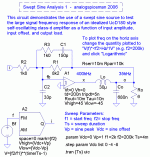
For all the LTspice aficionados out there, here are my recommendations of how best to use LTspice to optimize the feedback and control portions of your self-oscillating class-d designs.
- Don't run a full up simulation for this purpose - it just greatly increases run times and adds little of value to the optimization process.
- But do use the measured (or full up simulation) power stage delay as a realistic value to be entered as the delay parameter in the simplified power stage (explained below).
The power stage is essentially modeled as a power comparator with delay. Introducing a realistic delay is critical for predicting self oscillation frequency accurately. The diffschmitbuf A-device, one of LTspice's custom model types, is suited perfectly to this purpose (it even looks like a comparator). But first it must be set up by entering the following parameters (right mouse click over the device):
- Vt=0 Vh=0 ; sets input threshold and hysteresis voltage to zero to model an ideal comparator characteristic.
- Td=<delay> tripdt=1ns to Td ; sets delay value and accuracy band for switching edges (accurately bracketing transitions is critical for useful THD simulations).
- Vhigh=<+Vs> Vlow=<-Vs> ; sets the output rail voltages.
- Rout=<Rdson> ; typically set to equal output mosfet on-resistance.
- Tau=<Tt> ; transition time constant - set this to about one half the actual output stage 90%/10% transition time.
Note that this A-device does not model power supply interactions at all (not normally of interest during the control loop design phase). Fortunately, this can be added, if desired, at only a small cost to run times. (Do this via a totem pole pair of voltage controlled switch devices tacked onto the output of the A-device.)
Because this ideal A-device has infinite gain, LTspice will not be able to find an initial linear operating point, so "Skip Initial Operating Point Solution" (uic) must be specified in the Simulation Command panel.
- If you are comfortable with the frequency domain, an ac analysis can be used to set the component values in the feedback network. For this type of analysis replace the A-device with a voltage source (dc=0) followed by an Ideal Losses Transmission Line (tline) as a delay generator. The voltage source should have its small signal ac amplitude set to 1 (advanced menu) and its series resistance set to mosfet Rdson. For the tline, set Td to the power stage delay time and set Zo to mosfet Rdson.
If you are working with a UcD style feedback network, this analysis can be very helpful for ensuring that the lead network in the feedback path provides enough phase lead margin around the resonant point of the LC output filter operating into an open circuit.
The attached image show an example of the above applied to an LTspice analysis of a UcD style amplifier.
Attachments
- Status
- Not open for further replies.
- Home
- Amplifiers
- Class D
- Is the UcD modulation scheme less than optimum?