That right channel is way messed up. But you knew that.
With 10 volts on Q3 gate, if the transistor is any good, it should be almost hard saturated. The output should be +18 volts.
However, with that much voltage on the output the differential should be trying to shut that transistor off, not drive it off the board.
I'm too tired to look up the threshold voltage for these power fets, but Q6 maybe should be in cutoff, which is okay since there's no current on R16.
So you have at least 2 separate problems unless there is a short causing both.
I would attempt to isolate the current source around Q6 and make it work by itself if possible. You don't need a working amp for that.
Then I'd try to figure out why the differential is doing the exact opposite of what it should be doing. I'd check JFET gate voltages to make sense of their source currents. If Q1 gate is at 0 volts by normal R8 and connections, there is no way Q5 is off so long as any of the output voltage is making it through R2. Either the output voltage is in a different state than presumed or there is bad wiring or parts in the input or feedback loop. You said the JFETs were known to be good.
What is the current on R12?
Last edited:
You said the output was at 15 volts earlier, but you didn't specify polarity. Most of what you're describing would happen if the output was at -15 volts. You can't have a working output current source with no voltage across it. With all these tested good transistors, it's starting to sound like you have a bad connection between Q3 source and the + rail. Not much to check there. 🙂
Good morning EVeryone.
Hi Andrew, I've just woken up and seen your posts - thanks for the suggestions. I have just checked the connection between Q3 source and + rail, and it seems OK, although I'll have to take the board off again to see if there is anything underneath causing some kind of intermittent fault.
Actually, I think I'm going to measure voltages at all nodes (well, all easily accessible nodes) and will post back here shortly.
Cheers
Nigel
Hi Andrew, I've just woken up and seen your posts - thanks for the suggestions. I have just checked the connection between Q3 source and + rail, and it seems OK, although I'll have to take the board off again to see if there is anything underneath causing some kind of intermittent fault.
You said the output was at 15 volts earlier, but you didn't specify polarity. Most of what you're describing would happen if the output was at -15 volts. You can't have a working output current source with no voltage across it. With all these tested good transistors, it's starting to sound like you have a bad connection between Q3 source and the + rail. Not much to check there. 🙂
Actually, I think I'm going to measure voltages at all nodes (well, all easily accessible nodes) and will post back here shortly.
Cheers
Nigel
Hi Guys,
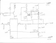
Well I've found one of the problems - but it was caused by me "fixing" things last night, and can't have caused the original problem. I've attached a scan of the schematic without component values but with voltages at several of the nodes. The ones not in parentheses are the first ones, the others in parentheses are a second measurement after fixing the error. As you can see, the voltage on the gate of Q6 didn't even nearly match the voltage on the collector of Q8, so Q6 wasn't switched on, and as a result many of the other voltages were out of whack. I took the board off and found the connection between R21 and Q8 wasn't conducting properly. This is clearly a mistake I made last night when I took the trimpot out and out a fixed resistor in its place for R15, because if it had been wrong originally the amp would never have worked, so it can't have caused the original problem.
It means, however, that the voltages I posted above don't mean anything with regard to the original problem.
The second set of voltage measurements (the ones in parentheses) seem to be OK, and right now the amp ois showing a DC ofset of just -20mV (which I can't reduce until the amp is put back together properly) so it seems everything is OK again. (Although I havn't played any music through it yet).
Of course I *still* don't know what has caused this intermittent problem. My best guess is that it was something wrong with the trimpot, but this is only a guess. I'm going to switch the trimpot out of the other channel also, I think, just to be on the safe side.
In hindsight I really should have done a voltage check at all nodes before changing anything, then maybe I would understand what was wrong. As it is, if anyone has any other guesses on what is causing this intermittent problem please let me know, since what has happened three times may well happen again, if the trimpot wasn't the cause...
Cheers
Nigel
....So you have at least 2 separate problems unless there is a short causing both.
Well I've found one of the problems - but it was caused by me "fixing" things last night, and can't have caused the original problem. I've attached a scan of the schematic without component values but with voltages at several of the nodes. The ones not in parentheses are the first ones, the others in parentheses are a second measurement after fixing the error. As you can see, the voltage on the gate of Q6 didn't even nearly match the voltage on the collector of Q8, so Q6 wasn't switched on, and as a result many of the other voltages were out of whack. I took the board off and found the connection between R21 and Q8 wasn't conducting properly. This is clearly a mistake I made last night when I took the trimpot out and out a fixed resistor in its place for R15, because if it had been wrong originally the amp would never have worked, so it can't have caused the original problem.
It means, however, that the voltages I posted above don't mean anything with regard to the original problem.
The second set of voltage measurements (the ones in parentheses) seem to be OK, and right now the amp ois showing a DC ofset of just -20mV (which I can't reduce until the amp is put back together properly) so it seems everything is OK again. (Although I havn't played any music through it yet).
Of course I *still* don't know what has caused this intermittent problem. My best guess is that it was something wrong with the trimpot, but this is only a guess. I'm going to switch the trimpot out of the other channel also, I think, just to be on the safe side.
In hindsight I really should have done a voltage check at all nodes before changing anything, then maybe I would understand what was wrong. As it is, if anyone has any other guesses on what is causing this intermittent problem please let me know, since what has happened three times may well happen again, if the trimpot wasn't the cause...
Cheers
Nigel
Attachments
Glad to see you mainly got it for now. This circuit is plain enough that measuring voltages should quickly lead to an understandable condition. You had to have had a connection failure or really weird part to get the situation you had.
If anything goes wrong with the trimpot, unless you dump metal flakes into it, the output should swing negative. If it breaks again, don't change nothin, just measure. 🙂
If anything goes wrong with the trimpot, unless you dump metal flakes into it, the output should swing negative. If it breaks again, don't change nothin, just measure. 🙂
Amp is back in the system, and playing beautifully. Yay!!!
You can be sure that if anything goes wrong again I'll plot out all the voltages before "fixing" anything. The trimpots for R15 won't be a problem now, though, even if they were before, since they are history. Pity I still don't understand what happened, but that's life, I guess...
Many thanks to everyone for your help.
Cheers
Nigel
Glad to see you mainly got it for now. This circuit is plain enough that measuring voltages should quickly lead to an understandable condition. You had to have had a connection failure or really weird part to get the situation you had.
If anything goes wrong with the trimpot, unless you dump metal flakes into it, the output should swing negative. If it breaks again, don't change nothin, just measure. 🙂
You can be sure that if anything goes wrong again I'll plot out all the voltages before "fixing" anything. The trimpots for R15 won't be a problem now, though, even if they were before, since they are history. Pity I still don't understand what happened, but that's life, I guess...
Many thanks to everyone for your help.
Cheers
Nigel
Have a laugh at my expense!
I think I've finally solved the odd amp-failure problem.... Here's what happened, and feel free to have a smile or laugh at my expense if you like... 😀
A couple of nights ago the amp failed again, exactly the same way as before, showing 16v of dc offset on the right channel. I took the heatsink off so that I could measure a few voltages, and when things magically went back to normal I put everything back together and decided to wait and see what would happen.
This morning it happened again, so I took the heatsink off again, and at the moment I measured dc offset the speaker protection circuit turned the output on (relay activated, blue LED lit up...) When I put the heatsink back on nothing happened - no relay, LED, nothing... So I repeated the process, with the same result - with the heatsink off, nothing happened until I measured dc offset, when it clicked on; with the heatsink off nothing happened at all, whatever I did. Just to be sure I repeated the process four or five times, with exactly the same result.
So I thought maybe some wire connecting to the protection circuit was dodgy, and being pushed or pulled somehow when I put the heatsink back on, but nothing was visible.
So I took the heatsink off again and the same thing happened again... measured DC offset and it clicked on. Just to see what would happen I flicked the board with my fingernail, and the thing clicked off immediately with a "pop" in the speakers, and then wouldn't click back on whatever I did. Clearly a physical problem with the board. A little invesigation with a DMM and I found that the connection to the drain of Q3 had failed. (Not Q6, which was the mosfet I *thought* was causing the trouble, as related above...)
In retrospect, it is clear what was happening. Like many small amp boards, it is supported by the pins on the mosfets (which are screwed into the heatsinks). Obviously the solder joint on the drain of Q3 was bad, and when in vertical position the weight of the board was stressing the joint, causing it to give a bad contact, and hence a large dc offset on the output. Once horizontal (after taking the heatsinks off) just touching the board to check dc offset was enough for the two parts to join, making the circuit and letting it click on. Flicking the board had caused the joint to fail completely, hence letting me find the problem. 😱 I should add, the joint didn't *look* bad, and of course measured just fine whenever I tested it, since the board was in horizontal position, so it wouldn't have been easy to find, but nonetheless... 😱
I can't reconstruct the original failure after so much time, and since I replaced Q3 after the first failure it may not have been the cause, but it seems likely to me that this was behind all other cases of the amp failure related above. So a big apology to everyone for not finding my newbie bad solder joint, but many thanks to you all for helping out with finding the problem. (And of course special thanks to juma for the original schematic and for repeated help...)
Cheers
Nigel
... Pity I still don't understand what happened, but that's life, I guess...
I think I've finally solved the odd amp-failure problem.... Here's what happened, and feel free to have a smile or laugh at my expense if you like... 😀
A couple of nights ago the amp failed again, exactly the same way as before, showing 16v of dc offset on the right channel. I took the heatsink off so that I could measure a few voltages, and when things magically went back to normal I put everything back together and decided to wait and see what would happen.
This morning it happened again, so I took the heatsink off again, and at the moment I measured dc offset the speaker protection circuit turned the output on (relay activated, blue LED lit up...) When I put the heatsink back on nothing happened - no relay, LED, nothing... So I repeated the process, with the same result - with the heatsink off, nothing happened until I measured dc offset, when it clicked on; with the heatsink off nothing happened at all, whatever I did. Just to be sure I repeated the process four or five times, with exactly the same result.
So I thought maybe some wire connecting to the protection circuit was dodgy, and being pushed or pulled somehow when I put the heatsink back on, but nothing was visible.
So I took the heatsink off again and the same thing happened again... measured DC offset and it clicked on. Just to see what would happen I flicked the board with my fingernail, and the thing clicked off immediately with a "pop" in the speakers, and then wouldn't click back on whatever I did. Clearly a physical problem with the board. A little invesigation with a DMM and I found that the connection to the drain of Q3 had failed. (Not Q6, which was the mosfet I *thought* was causing the trouble, as related above...)
In retrospect, it is clear what was happening. Like many small amp boards, it is supported by the pins on the mosfets (which are screwed into the heatsinks). Obviously the solder joint on the drain of Q3 was bad, and when in vertical position the weight of the board was stressing the joint, causing it to give a bad contact, and hence a large dc offset on the output. Once horizontal (after taking the heatsinks off) just touching the board to check dc offset was enough for the two parts to join, making the circuit and letting it click on. Flicking the board had caused the joint to fail completely, hence letting me find the problem. 😱 I should add, the joint didn't *look* bad, and of course measured just fine whenever I tested it, since the board was in horizontal position, so it wouldn't have been easy to find, but nonetheless... 😱
I can't reconstruct the original failure after so much time, and since I replaced Q3 after the first failure it may not have been the cause, but it seems likely to me that this was behind all other cases of the amp failure related above. So a big apology to everyone for not finding my newbie bad solder joint, but many thanks to you all for helping out with finding the problem. (And of course special thanks to juma for the original schematic and for repeated help...)
Cheers
Nigel
Thank you Nigel for not being too shy to expose your mistake (many guys are) 😉
For those who can use some help on basic stuff and are reluctant to read long posts:
Always make sure that your solder joints are electricaly and mechanicaly good !
For those who can use some help on basic stuff and are reluctant to read long posts:
Always make sure that your solder joints are electricaly and mechanicaly good !
Hi Guys,
Well, I'm not sure I can do this retroactively, so to speak, without stressing the joints worse. But you can be sure I'll remember for next time! (Maybe it's worth the trouble to redesign and rebuild the boards completely, actually... we'll see...)
Really three mistakes.
1. Bad joint: Electrically OK, but mechanically too weak for what was required. I should have caught this in the first place.
2. Bad design, not supporting the board separately from the mosfet pins.
3. When searching for the problem, assuming that the problem was where I thought it was (Q6), when it was actually somewhere else (Q3)...
I don't mind sharing my mistakes. I can't contribute much to the technical aspects of the forum, but at least I can let people know what the problem was after they were kind enough to help me look for it!
Thanks again
Nigel
point is - doesn't matter how small is - always fix pcb
😉
Well, I'm not sure I can do this retroactively, so to speak, without stressing the joints worse. But you can be sure I'll remember for next time! (Maybe it's worth the trouble to redesign and rebuild the boards completely, actually... we'll see...)
Thank you Nigel for not being too shy to expose your mistake (many guys are) 😉
Really three mistakes.
1. Bad joint: Electrically OK, but mechanically too weak for what was required. I should have caught this in the first place.
2. Bad design, not supporting the board separately from the mosfet pins.
3. When searching for the problem, assuming that the problem was where I thought it was (Q6), when it was actually somewhere else (Q3)...
I don't mind sharing my mistakes. I can't contribute much to the technical aspects of the forum, but at least I can let people know what the problem was after they were kind enough to help me look for it!
Thanks again
Nigel
.....
I don't mind sharing my mistakes. ........
even in case that you keep them coming for decade or so , you can't touch my silliness ratio .....

Happy Happy Day
Hi Nigel
Very happy for you in that you've found the source of the problem.🙂
In my past work with DC-coupled amps, for difficult problems I would have opened the feedback loop to see if the problem was not being caused elsewhere, as you have discovered that Q6 was not at fault but rather the Q3 was.
When I examined your schematic I was not sure how this could have been done without causing other undesirable (DC) bias effects.
So I put the question to those familiar with this design how you/they might be able to open the negative FB loop while still maintaining the DC operating values?
Cheers
Philip
Hi Philip,
I don't understand what you mean. That is, I know what you mean by "open the negative feedback loop", but I don't see how that would help. Can you give an example from a different schematic?
Cheers
NIgel
I don't understand what you mean. That is, I know what you mean by "open the negative feedback loop", but I don't see how that would help. Can you give an example from a different schematic?
Cheers
NIgel
Hi Nigel
Sorry I don't have any pics I could post as I’m not currently at home.
But the theory works something like this.
Because the amp in question is based upon a negative feedback design other things are happening that are not directly related to the processing of the sound. For example, one of these things is that the amplifier is trying to maintain a value of zero volts at its output (typically seen when there is no signal input). This checking function is done by the differential (Long Tail Pair or LTP) FETs that make up the input stage of the amp. Should the negative (or inverting) input of the LTP see a voltage that is not present on the positive (or non-inverting) input, the LTP will try to correct this by forcing the amplifier to output a signal that is inversely proportional to the error voltage in an attempt to cancel the erroneous output value. In cases where an amplifier is producing unwanted noise from within the circuit, this debugging technique is probably the best way to discover the flakey part without having to change everything.
Now in your case the Q3 transistor was not doing its job because of the bad connection, this would have caused the output to vary a little away from its normal Zero set point, however because of this the LTP stepped in and applied the full gain of the amplifier in an attempt to correct the problem. This than resulted in the excessive drive signals you were seeing on the Q6 transistor, making it look like it was the faulty culprit.
So Nigel the small error voltages that the Q3 was generating that could have been used to show that it was bad was being swamped by the fully amplified correction signal that was being sent by the LTP forcing the Q6 to try to correct the situation. So it kind of makes sense that if you can prevent the LTP from overreacting to the fault you would have been able to trace the fault directly to its source.
Typically opening the feedback loop is done by either removing the feedback resistor that monitors the output signal or by shorting the gain setting resistor that follows the FB resistor into the LTP. In other cases you can place a very large capacitor across this gain setting resistor to simulate a short but I question whether this would have worked in your circuit.
So that’s where my question comes from, “how do we open the loop on this amp”?
Cheers
Philip
hi there,
i built one channel of the amp and i think one bf862 in the diff pair blew up. now i m kind of tired of handling those little jfets. i guess i can use some 2sk170 instead? what bias should they be ran at? 2ma?
i built one channel of the amp and i think one bf862 in the diff pair blew up. now i m kind of tired of handling those little jfets. i guess i can use some 2sk170 instead? what bias should they be ran at? 2ma?
hi there,
i built one channel of the amp and i think one bf862 in the diff pair blew up. now i m kind of tired of handling those little jfets. i guess i can use some 2sk170 instead? what bias should they be ran at? 2ma?
You can use k170 in diff. pair and they run at about 9mA each. So you should use JFETs with Idss in range of 12-15mA.
thank you Juma,
listening right now to the amp, it s realy nice. nothing to compare with right now but after it warms up it s pretty top.
why exactly does the jfets prefer 9ma in this topology? i m currently in the process of learning more how what i build works.
also would the output stage of the mini-a be fitted in this schematic to power speakers directly? i guess without feedback...?
it was taken from raylectronics.nl
Attachments
Last edited:
pidesd,
JFETs don't prefer Id of 9mA - we do. For BF862 or k170BL (with Idss in range of 12-15mA) that's the region where transfer characteristic is linear. That's the way to use them in order to make them sound nice. For some other JFETs it will be some other value...
Find Erno Borbely's articles (JFET Frontiers 1 and 2) and study them.
The schematic you attached is not what I consider good circuit. JFET's Id is way too small and CFP (T1a/b and T2a/b) is not what sounds good to my ears. Also, it can't be easily used as power amp without feedback loop. With some effort it can be done but it will sound inferior to what you have now.
''JFETs don't prefer Id of 9mA - we do''
i think we understand each other, but you are right 🙂
about that linear thing, i began looking at this and graphs but they hardly look ''linear'' to me. i guess i ll have to read the articles, thank you for pointing me to them.
''sound inferior to what you have now''
i guess you mean a normal output stage with amp VS what i m suggesting.
why do you think that the input stage shown (with or without CFP) when not starved coupled to the aleph output stage with feedback would not be very good?
i believe i may not understand right now, but i kind of like the idea and sound of simple circuitry.
anyway...i ll look more into this...
by the way i ll try to upload pics of what i have done, it sounds really good, thanks for sharing, Juma
Last edited:
- Status
- Not open for further replies.
- Home
- Amplifiers
- Pass Labs
- Is a mini-Aleph using BF862 possible?