Another thing that I keep forgetting to mention is, IMHO when it comes to sound (not THD numbers), we better used simple (DC coupled preferable) J-FET buffer either single-ended or push-pull than an opamp wired as a buffer, they often sound bad that way.
how come we don't see those J-FETs on the PCB or the schematic?
3 or 4 board solution for a simple stereo amp is a luxury, yes
IMO a more challenging engineering task is to put all the amplifiers and PS on a single PCB /one sided for compact, competitive costs, yet still sounds good.
Last edited:
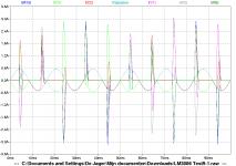
A ground plane with 6 caps, 1 speaker return and 1 supply return will have 9 charging currents and 7 speaker currents. Add to that ground loops and ground connections, it all becomes very uncontrollable.
how come we don't see those J-FETs on the PCB or the schematic?
'Cos that particular pcb is not design for buffer usage.
IMO a more challenging engineering task is to put all the amplifiers and PS on a single PCB /one sided for compact, competitive costs, yet still sounds good.
The real challenge IMHO is to squeeze max. performance from the LM3886...To do that one should not skimp on the wrong places.
A little math for you: could your estimate how much it would cost making only one pcb relative to the value of the power supply unit that you previously stated intend to used?
A ground plane with 6 caps, 1 speaker return and 1 supply return will have 9 charging currents and 7 speaker currents. Add to that ground loops and ground connections, it all becomes very uncontrollable.
Mark, if everything is as you say when it comes to current loops control , probably you could not even write what you wrote, because you PC would stop working.😀
Last edited:
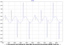
A classic class B output stage switching distortion (and harmonics)...The same current will flow through be it ground wire or ground plane, it's loop they have to travel we are interested in. Do you see a little cap that is connected between amp PSU pins in psb that I proposed previously...do you understand its role?
'Cos that particular pcb is not design for buffer usage.
The real challenge IMHO is to squeeze max. performance from the LM3886...To do that one should not skimp on the wrong places.
A little math for you: could your estimate how much it would cost making only one pcb relative to the value of the power supply unit that you previously stated intend to used?
my original Q about your buffers remains?
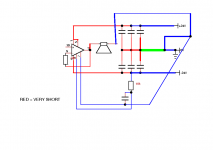
your image of a much lower power and simpler circuit is offered as a solution to a buffered LM3886, I don't think so.
I offered no solution , just a cautionary warning on the 1st important PCB design decision. eg Wide power traces are good but a sensitive ground plane beneath them can be corrupted.
the total BOM cost is carefully weighed against electrical performance in all aspects. The XFMR/ PS size one chooses is not a gauge of the PCB cost, for every penny will add up to much on high volumes.
my original Q about your buffers remains?
And that would be...?
your image of a much lower power and simpler circuit is offered as a solution to a buffered LM3886, I don't think so.
I do not suggest (and I never suggested) that the schematic is better than buffered LM3886, it's not. What I suggested is how ground plane and the signal lines should be routed on a 2-layer board. If you don't like it, don't use it, it's that simple.
The XFMR/ PS size one chooses is not a gauge of the PCB cost, for every penny will add up to much on high volumes.
So, it's ok for you to spend 200-300$ for PSU, but spending 20$ for a psb is no-no😕
As I said earlier, you do not have to use "proper" PCB, you can use the prototype pcb, rotate LM3886 by 45° so the pins fine snugly into the holes, and use p2p wirering...it will be an order of magnitude better then badly design one.
As I show in the LM3886 P2P vs PCB thread, it is perfectly possible to screw up a P2P layout. It's noteworthy that moving two connections in the P2P setup changed the performance from "utter crap" to "stellar".
What a PCB gives you above all is repeatability. So if you have a good layout, you will get good performance for every unit you build. But if the layout is crappy, you'll get crappy performance for every unit you build.
~Tom
What a PCB gives you above all is repeatability. So if you have a good layout, you will get good performance for every unit you build. But if the layout is crappy, you'll get crappy performance for every unit you build.
~Tom
Hi all,
Second try at the PCB layout, the Zobel path is short as possible, the 15 Ohm part of the Zobel network is under the board, decoupling capacitors as close as possible to the chips (LM3886 and the LME49710). Most of Tom's advice has been taken into consideration, so any opinions are welcome.🙂
Best regards.
Second try at the PCB layout, the Zobel path is short as possible, the 15 Ohm part of the Zobel network is under the board, decoupling capacitors as close as possible to the chips (LM3886 and the LME49710). Most of Tom's advice has been taken into consideration, so any opinions are welcome.🙂
An externally hosted image should be here but it was not working when we last tested it.
Best regards.
Hi sghr220,
Read the TI data sheet for the LM3886, Chapter: LAYOUT, GROUND LOOPS AND STABILITY.
Clear explanation why not to use ground planes and what the result will be if you do.
Read the TI data sheet for the LM3886, Chapter: LAYOUT, GROUND LOOPS AND STABILITY.
Clear explanation why not to use ground planes and what the result will be if you do.
Last edited:
Mark,
I think that depends entirely on how you design the ground plane. You could have a ground pour for the high currents and return the low currents (FB, input) through separate traces connecting to the ground plane at the star ground.
I'm toying with the idea of having VCC, VEE run side-by-side on the top layer as pours from the power in connector to the IC with GND on the bottom layer. The GND plane would extend to cover the same area as the VCC, VEE planes. That should ensure that the return currents flow in the ground plane below the VCC and VEE planes respectively. I would route Vout as a pour on the top layer with Vout_GND routed as a plane directly below it on the bottom layer. Now you have control of the load current as well. The only thing left at that point is to manage the input and feedback grounds. They'd be traces on the top and I might have to have a couple of keep-outs in the ground plane to ensure that their connections return through traces rather than the plane.
If the term "ground plane" bothers you, just think really, really wide traces... 🙂
The LM3886 data sheet does not say, "don't use a ground plane". It says, "pay attention to your ground routing". At least as I read it. You do need to heed the advice to get the full performance.
~Tom
Last edited:
Hi tomchr,
The problem with using planes is getting the speaker return and the charging currents correct. Try drawing the currents.
From the TI DS, "common ground point through separate paths", really does exclude a ground plane.
In your case you have a benchmark with the P2P version and if you can build a better PCB version that would be great.
Hi all,
My juvenile approach to star grounding 🙂.
Best regards.
My juvenile approach to star grounding 🙂.
An externally hosted image should be here but it was not working when we last tested it.
Best regards.
Sorry, didn't edit on time limit so here is a semi-final version.
An externally hosted image should be here but it was not working when we last tested it.
Best regards.
- Status
- Not open for further replies.
- Home
- Amplifiers
- Chip Amps
- Inverting LM3886


