Why is a ground plane of no use? It minimizes the ground impedance (including inductance if my understanding is correct). Isn't that what we want?
~Tom
You did not use a ground plane with your prototype and you got great results, why do it differently now.
You did not use a ground plane with your prototype and you got great results, why do it differently now.
I guess Tom did use a ground plane in his PCB, not sure really.
Why is a ground plane of no use? It minimizes the ground impedance (including inductance if my understanding is correct). Isn't that what we want?
I should have been clearer, ground plane on a single layer PCB is of no use for a power amp like this one. A ground plane to correctly played its role would have to be continuous, not intersected with pads and lines. If it's not continuous, circulating current form various points in circuit would have to travel longer, some of them via least impedance path (LF), some of them via least inductance path (HF). In any case, we lose the ability to control these paths-loops, which will be happy to radiate exactly where we do not want, or receive interference where we do not want. So, if we have the ability to control this paths, be it p2p wiring or lineas in PCB, my best advice is to take advantage an use it.🙂

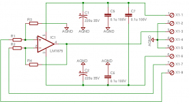
Hi all,
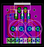
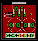
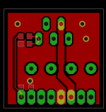
Here are the first attempt at the board layout (one channel) along with the last updated schematic, your input would be most welcome.🙂
Hi sghr220,
It looks like you are using Eagle for the PCB. Did you redraw the schematic in Eagle? [If not, IMO it is extremely important to have the schematic and PCB in the one application. Back and forward annotation and net checking are vital to your chances of a successful project.]
regards
If you want to know what is wrong with ground plains, just follow the currents.
Exactly!

Hi sghr220,It looks like you are using Eagle for the PCB. Did you redraw the schematic in Eagle? [If not, IMO it is extremely important to have the schematic and PCB in the one application. Back and forward annotation and net checking are vital to your chances of a successful project.]regards.
Thanks for the advice Greg, will use Eagle (or Proteus) for both the schematic and the layout in future projects.
Best regards.
Can i use a jumper wire in this area or is it too sensitive?
The key with the Zobel network is that its inductance needs to be minimized. I think you can do a better job at that than what's shown in your initial layout. It may mean that the C gets closer to the chip and the R connects to ground. You'll have to play with the parts placement to figure out what works.
I don't fully understand that but i'll try to get the Vee 100nF decoupling closer to the chip.
That's because I mistyped. Scoot up the VEE cap. Rotate the VCC cap 90 degrees. The goal is to get the supply side of the cap as close to the IC pins as you can.
Thermal relief on the pads connecting the two ground planes?
Thermal relief on all pads connecting to the ground plane. Unless you have a good soldering iron that's capable of heating up both the component lead and the ground plane enough to make a good connection.
- Mounting holes will be added in the final version and copper standoffs will be used to provide clearance.
Copper standoffs. Ooh. Fancy!
- Will bring the chip closer to the board edge but Rmute has very small effect on the heat sink mounting either vertically or horizontally.
As long as it fits.
~Tom
You did not use a ground plane with your prototype and you got great results, why do it differently now.
Actually, I did. The ground plane was added late, hence, is on the top layer (green). I might be able to eek out a little more performance by moving it to the bottom layer (red). Note that - as mentioned many times now - this layout is ***NOT*** optimal. I've learned quite a bit since I made this board. I need to transfer those learnings to the PCB - and probably spend more than the 45 minutes it took me to draw the board shown below. I've grayed out irrelevant bits of the design.

Ground plane currents can be tamed by breaking up the ground plane. That gives you control of where the current flows.
~Tom
Last edited:
For the ground current: By designing the ground plane to make the current flow where you want it to. Be careful not to have too many choke points in the ground plane.
VCC,VEE currents can be tamed by the trace routes. I would be tempted to pour the ground on the bottom layer and have VCC,VEE run as pours from the input connector all the way up to the IC pins.
I plan to work on my PCB over the weekend. I can post screen shots of the relevant portions if you'd like. That way we can both feed off each other and have good layouts.
~Tom

OK Tom, since you're determine to use a ground plane(s), here are few examples how to do it right from the start... Rule No. 1 .. use 2-layer board😉
first image - schematic
second image - overall layout
third image - top layout
forth image - bottom layout
fifth image - solder stop layout
first image - schematic
second image - overall layout
third image - top layout
forth image - bottom layout
fifth image - solder stop layout
Attachments

Nice... And yeah... I always use two-layer boards. Even in my home "fab" I can usually get the registration between top and bottom layer down around 0.2 mm. Good enough for leaded parts for sure.
~Tom
~Tom
Maybe the amp would have been even better without connecting all those planes together?
I cant help comparing a ground plane to the atmosphere of our planet. 100 tropical storms every second, scary place to be.
I cant help comparing a ground plane to the atmosphere of our planet. 100 tropical storms every second, scary place to be.
good analogy Mark
unless you have a really good reason for a ground plane, don't do it esp on a switched power PCB. just more work and too many gotchas await.
unless you have a really good reason for a ground plane, don't do it esp on a switched power PCB. just more work and too many gotchas await.
Maybe the amp would have been even better without connecting all those planes together?
I cant help comparing a ground plane to the atmosphere of our planet. 100 tropical storms every second, scary place to be.
No, one have to understand why and how ac currents flow in an amp/pcb. And its more like a breeze if you know what you're doing.🙂
Another thing that I keep forgetting to mention is, IMHO when it comes to sound (not THD numbers), we better used simple (DC coupled preferable) J-FET buffer either single-ended or push-pull than an opamp wired as a buffer, they often sound bad that way.
- Status
- Not open for further replies.
- Home
- Amplifiers
- Chip Amps
- Inverting LM3886