This is just a demo to show what I mean, it still needs some tweaking and I would run some sims before making this.
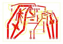
I cheated a bit by using 2 PSU and I still need to work out the 0V connections between the two PSU.
The Speaker is connected to the trace at pin 3 and the return is connected to 0V star.
I cheated a bit by using 2 PSU and I still need to work out the 0V connections between the two PSU.
The Speaker is connected to the trace at pin 3 and the return is connected to 0V star.
Attachments
Last edited:
Mark, you are missing HF decoupling capacitors for the LM3886 and opamp. Also, a star at star-ground term (and real pcb), means a POINT rather than surface from which the lines on the pcb emanating from. The lines that goes to decoupling capacitor pins should be so thick that the AC current going TO the pins, not around them.
HF decoupling caps are on the underside of the PCB and can be rail to rail and/or rail to 0V.
Most designs only place the HF decoupling caps close to the supply pins and then place the speaker return on the other end of the PCB. The HF current must return to the HF caps to be effective.
This design study is implementing TI data sheet guidelines, as I see them and tested with P2P. It could be improved by redesigning as a 2 layer PCB.
Last edited:
HF decoupling caps are on the underside of the PCB and can be rail to rail and/or rail to 0V.
Ok then, I could not see them.
Most designs only place the HF decoupling caps close to the supply pins and then place the speaker return on the other end of the PCB. The HF current must return to the HF caps to be effective.
Right, that's what I'm saying right from the start.
Another update 🙂, at the moment i can't think of further improvements so your opinions are welcome.
P.S. I almost reverse engineered Tom's board so thank you Tom for your patience and all your good advice.
Best regards.
P.S. I almost reverse engineered Tom's board so thank you Tom for your patience and all your good advice.
An externally hosted image should be here but it was not working when we last tested it.
Best regards.
.jpg")

A quick one...
And then place the speaker return and zobel return at the centre of the star.
I think you're both wrong, here is why...
The positive and negative rail reservoir caps will be joined together by a thick earth connection; this is called reservoir ground (RG). Do not attempt to use any point on this track as the audio-ground star-point, as it carries heavy charging pulses and will induce ripple into the signal. Instead take a thick tee from the center of this track (through which the charging pulses will not flow) and use the end of this as the star-point.
Audio Power Amplifier Design Handbook, Douglas Self, 5th edition.
Do your homework gents. 😛
Quite the opposite, you have to do your homework, 'cos you don't know what is reservoir ground (RG)...let me help you - it is right in the middle of your bulk capacitors.
sghr220,
have you not returned the speaker return and the zobel return to the reservoir ground?
Maybe you could post some links of PCB's using this method.
have you not returned the speaker return and the zobel return to the reservoir ground?
Maybe you could post some links of PCB's using this method.
Last edited:
sghr220,
have you not returned the speaker return and the zobel return to the reservoir ground?
Maybe you could post some links of PCB's using this method.
Could you show me an LM3886 PCB (a real one) of your own design? same goes for the other fellow?😛

My design is exactly as Mr pass is describing.
This is my last attempt at showing you what I mean. I was just trying to help.
I just hope some of this is useful to others.
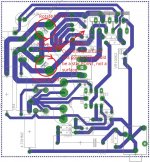
Okay people putting aside some lame comments and ego maniacal personalities, back to the main topic at last. My latest attempt at board layout is below, any productive advice is much appreciated. 
An externally hosted image should be here but it was not working when we last tested it.
The loop areas of the input side are far too big.
The HF and MF decoupling have traces that are far too long on both the chipamp and the opamp.
The HF and MF decoupling have traces that are far too long on both the chipamp and the opamp.
Member
Joined 2009
Paid Member
any productive advice is much appreciated.
I'd say you have some very tight spacings between traces/pads carrying different signals which with some more careful thought could be improved on and will make the board more reliable to fabricate and solder. As to other aspects of the layout - there are already others who have more knowledge than me that have offered their input - even if the language of their input is irritating to you it might not have been intended that way and it is worth reading carefully what they say and then making your own mind what to accept and what to reject.

sghr220. I would refer you back to post #105
All forum members have the right to post openly on the forums. If you do not wish to see replies from any individuals then add them to your "ignore list" in the user control panel options.
Other posts deleted.
Um, dude... Arguing with the ref is not a recipe for anything good. I saw your posts from yesterday and really had to bite my tongue. Communication is a two-way street. Just because you say something that's perfectly clear to you, doesn't mean it's received clearly. Regardless of the language proficiency of the communicators.
Now, on your layout, I suggest thinking through the loops like AndrewT hints at. For example, the supply for your LM3886: On VCC, the main current loops run from the decoupling caps through the IC back to the decoupling caps. Minimize the loop inductance by minimizing the loop area (L is proportional to the loop area). The main supply caps are less important here. You can live with a longer route as the bigger caps mainly supply the LF currents. All the high-speed stuff (if 1 MHz can be considered HS these days anyway 😉) takes place in the local decoupling.
Always remember: Signal flowing out has to return to the source somehow. Trace those routes and minimize their loop areas.
~Tom
Hi Tom,
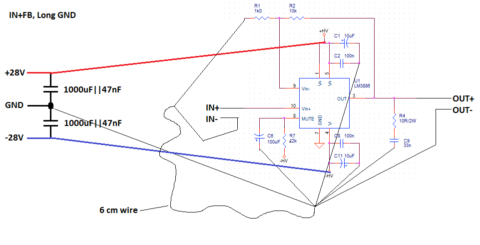
In the schematic above you took a wire from between the reservoir capacitors to the star ground also that's what i quoted from Douglas Self book and that's what i did in my last layout is something wrong with that?
Regarding long return routes...Is there any component placement advice you would like to add, How long is too long a route to the ground?
- Status
- Not open for further replies.
- Home
- Amplifiers
- Chip Amps
- Inverting LM3886