I've been curious about inverting vs non-inverting as well. I understand the theory behind it. If the common-mode voltage varies (as it does in the non-inverting configuration), there is potential for the introduction of common-mode related distortion products. So I ran a THD sweep. See attached.
interesting , so far I call it a draw, can your buffer drive 1K cleanly? most OP amps start to object to those loads
I wonder about PSRR since one V rail matches the CMMR and the other is 10 dB better.
lets hear it for 2 tone IMD testing 19 KHz + 20 KHz.
Last edited:
Just throwing a wrench in your works here. You're welcome, buddy...🙂
I've been curious about inverting vs non-inverting as well. I understand the theory behind it. If the common-mode voltage varies (as it does in the non-inverting configuration), there is potential for the introduction of common-mode related distortion products. So I ran a THD sweep. See attached.
The circuit is the "GND STAR" topology I posted last night in the LM3886 PCB vs P2P Thread, Post #30. For the inverting configuration I added an LME49710 buffer to drive the 1 kΩ input impedance of the inverting LM3886.
Note that the noise floor of my HP 8903A results in a reading of 0.0018~0.002 % THD+N, so basically, the two circuits are neck and neck with the test equipment until about 5 kHz when the inverting configuration shows slightly worse THD. I plan to retake the measurement using an AP SYS-2712 that I just happen to have access to... 🙂 Stay tuned.
~Tom
No problem Tom and thanks for the valuable contribution, as for the future tests could you please exclude the driver op amp (the LME49710) from the circuit as i believe for a meaningful results both the inverting and non inverting LM3886 configurations should be isolated from other factor (other components). 🙂
Best regards.
well thanks, I was beginning to wonder if my posts were invisible.
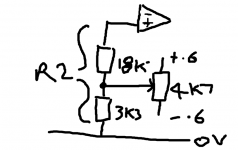
as I said post 29 there is a big mismatch between R2 and R4. with Ib bias is about 10 times Ios AND this resistor mismatch, this offset is huge, along with an unknown tempco factor.
The schem. in post 30 with my changes to Rb ~14K should be better all around. IMO
Also might consider at least doubling the input AC impedance to 2K.
yes the DC test circuit in the data sheet e.g. balanced 50 ohm inputs. > makes Vos dominate and very easy to measure with accuracy.
Hello there, i really appreciate your help and the time and effort you're taking to do so...so to avoid confusion (mine mostly 🙂) here is the schematic i am working on now after taking in much of the advice being offered and also an extract from the National's datasheet explaining how to determine the resistors values to achieve low DC offset. Could you point out what's the problem with the schematic chosen values?


Best regards
Listen 🙂
For minimum DC offset the currents flowing out of the two opamp inputs must be equal. In your circuit that means R2 must equal R4. R1 in your circuit has zero effect on the offset because there is no DC path through it.
In the other circuit I don't actually agree with what is written. The parallel combination is not 20k and 1k (the 953 ohms shown) but 20k + (1k + 47k) in parallel which is 14117 ohm.
Listen 🙂
For minimum DC offset the currents flowing out of the two opamp inputs must be equal. In your circuit that means R2 must equal R4. R1 in your circuit has zero effect on the offset because there is no DC path through it.
In the other circuit I don't actually agree with what is written. The parallel combination is not 20k and 1k (the 953 ohms shown) but 20k + (1k + 47k) in parallel which is 14117 ohm.
Thanks for the clarification Mooly 🙂, the source of confusion was definitely the datasheet, below is the updated schematic. One final (hope so) question: Should the RF cap be connected between the amplifier terminals or between the -ve terminal and the signal ground?

Noise with 220k attached to both +IN and -IN inputs will be higher than if the opamp sees 10k, or 1k, or 100r on it's two inputs.
As the frequencies go up the capacitors will allow a lower impedance.
What is the source impedance feeding this stage?
Does the source impedance vary, either with frequency, or with signal level?
As the frequencies go up the capacitors will allow a lower impedance.
What is the source impedance feeding this stage?
Does the source impedance vary, either with frequency, or with signal level?
big caps floating are a problem, it's possible to build up charges and cause clicks, pops, and even damage.
yes R4 R2 is getting higher than normal for a chip amp,
consider the alternate schematic with correctly calculated or trimmed Rb
yes R4 R2 is getting higher than normal for a chip amp,
consider the alternate schematic with correctly calculated or trimmed Rb
Noise is determined by the impedance seen from each input down to signal ground. The R4 220k has no influence on the noise. The 10k is the contributor.Noise with 220k attached to both +IN and -IN inputs will be higher than if the opamp sees 10k, or 1k, or 100r on it's two inputs.
The inverting configuration over at Decibel Dungeon just have +input to ground. Is DC offset biasing really a big problem with the LM3886?
Surely the 220K will go to ground eventually, but noise will come from 220K||10K which is so close to 10K we can ignore the 220KNoise is determined by the impedance seen from each input down to signal ground. The R4 220k has no influence on the noise. The 10k is the contributor.
Last edited:
The inverting configuration over at Decibel Dungeon just have +input to ground. Is DC offset biasing really a big problem with the LM3886?
Surely the 220K will go to ground eventually, but noise will come from 220K||10K which is so close to 10K we can ignore the 220K
people are reporting over 100mv DC mainly due to Vos, improper input biasing has the potential to at least double or triple that. IDK ask the OP if he is OK with DC output with no signal
Last edited:
Thanks for the clarification Mooly 🙂, the source of confusion was definitely the datasheet, below is the updated schematic. One final (hope so) question: Should the RF cap be connected between the amplifier terminals or between the -ve terminal and the signal ground?
Best regards.
What I would do is this...
Stick to the approximate value of feedback resistor in the data sheet examples, something like 22k being ideal, and 1k as an input resistor.
R2 needs to be a similar value to R4. Noise contribution from these values is low and if you bypass R2 with a cap it falls even further. A 22uf cap is plenty.
RF cap ? Not quite sure what you are referring to here. The common locations are across R4 (a small compensation cap perhaps as low as 10 to 50pf) and an input RF filter which is across the input and input ground. That's not as straightforward because you need to define impedances first, such as the source impedance driving the stage. I wouldn't worry over an input filter at the moment.
Connecting a small cap between the two amplifier inputs is something entirely different and reduces loop gain at a frequency determined by the cap.
The biggest problem you have is deciding how to drive this. The input impedance with optimal value parts for the power amp is low (1k). That's one of the downsides of the inverting configuration. Ideally you could have an inverting opamp stage driving a lowish value volume pot, say a 4.7k dual gang. Use a linear pot, these track better than log type and the input impedance of the amp (the low 1k) will alter the law of the pot closer to a log one. Any modern opamp such as an LM4562 will have no problem driving a 1k or lower load.
And one idea for trimming offset. Use two diodes to generate a -/+0.6 volt supply. That's just one resistor and diode across each rail. Connect a pot across this reference and use it to inject a current into a "split" R2. This should allow adjustment of the offset to zero. I've just guessed at typical values but it should be workable.
Attachments
What is the wideband source impedance connected to that 10k?
Is it a 100k vol pot? or a 100r low output impedance active stage?
Is it a 100k vol pot? or a 100r low output impedance active stage?
No problem Tom and thanks for the valuable contribution, as for the future tests could you please exclude the driver op amp (the LME49710) from the circuit as i believe for a meaningful results both the inverting and non inverting LM3886 configurations should be isolated from other factor (other components). 🙂
I did actually run the test with no driving op-amp at first, but my HP8903A cannot deliver the needed 2 V swing into a 1 kΩ load cleanly. The input impedance in my circuit is 1 kΩ because the feedback network I use is 10k, 1k. I did not test to see if the AP would drive 1 kΩ directly as I already had the buffer in place.
The LME49710 delivers a 3 V RMS swing into a 600 Ω load at 0.00003 % THD. I will not - repeat NOT impact the measurement of the LM3886. That's the whole point. Using a buffer that is strong enough to drive the input impedance is the only way to get meaningful data. Now, to get this performance, you have to be very careful with the layout, in particular with the ground connection between the LME49710 and the LM3886.
See attached data. For the inverting configuration, I drove the LM3886 with the LME49710. For the non-inverting, I drove the LM3886 directly. The THD is dominated by the LM3886 in both cases (by at least two orders of magnitude).
~Tom
Attachments

See attached data. For the inverting configuration, I drove the LM3886 with the LME49710. For the non-inverting, I drove the LM3886 directly. The THD is dominated by the LM3886 in both cases (by at least two orders of magnitude).
~Tom
That's really some revealing data Tom, so the message sent by that last graph is that between 20~200 Hz they're both have equal performance but above that the non-inverting standard configuration is actually better. One question remains though...why is your circuit , the "something better" 🙂 revolves around the inverting configuration whilst it requires additional components (LME49710) and careful layout? was that for experimentation purpose or just playing around with different chip amp configurations?
Best regards.
One question remains though...why is your circuit , the "something better" 🙂 revolves around the inverting configuration whilst it requires additional components (LME49710) and careful layout? was that for experimentation purpose or just playing around with different chip amp configurations?
I think you're referring to the circuit I hinted at in the LM3886 PCB vs P2P Thread. My New and Improved take on the LM3886 uses a low-THD op-amp to control the LM3886, thereby, reducing its distortion. Ideally, it should lower the THD to that of the controlling op-amp (so figure an LM3886 on steroids delivering 0.00003 % THD at 1 kHz, full power). The new circuit is a challenge to design - both due to the vanishingly low THD and due to stability, so I figured I'd build a prototype using P2P wiring.
My interest in inverting vs non-inverting configuration was driven by this project need. In the past, measuring regular op-amps, I've actually found that the non-inverting configuration provided the best performance. But that was one amp (LMP8100). I was curious to see if the THD was in fact lower in the inverting configuration or if it was just one of those "someone on the Internet said..." types of situations. It turns out the inverting configuration does provide better performance at higher frequencies. I doubt it will result in a perceived difference in sound quality, but it does measure better performance.
Now, the more interesting question in my mind is whether the inverting configuration is worth the extra trouble to deal with its low input impedance. Even 10 kΩ is kinda low, but probably OK - unless you use a volume pot, then you will need a buffer. I don't like the resulting 200 kΩ feedback impedance, though. Even the 10 kΩ I'm using will show up in the output noise. So given that I've painted myself into the low impedance corner for noise reasons, I am forced to use an op-amp driver. This adds cost and complexity (and plenty of opportunities to screw up and actually get much, much worse measured THD performance).
In my "LM3886 on Steroids" circuit, I would likely need two extra op-amps to have the LM3886 be inverting as the inverting LM3886 would mess up the stability of the overall circuit. So one more op-amp to invert and another op-amp to drive the resulting low input impedance. Not worth the trouble, I think. In my circuit, the THD should be dominated by the driving op-amp, so you would never see the difference between the LM3886 inverting/non-inverting as that effect is reduced by some 50-ish dB (assuming theory holds).
Personally, if I was a DIYer without any test gear to verify my build, I would build the non-inverting configuration and move on.
Given that I have access to some kick-a** gear, I choose to implement the circuit to deliver the best performance. I then put the circuit on a PCB such that others can buy my PCB and get the same performance as I get (assuming they stick to the parts on the BOM).
I'll post my LM3886 on Steroids circuit in a separate thread once it's ready for prime time.
~Tom
@ infinia, tomchr, Mooly, Ashok, peranders and Robert Kesh....
Thanks to all of you for your valuable contribution to this thread but despite the somehow contradictory information and points of view i've decided to go with the design in post #45 after some minor modifications shown below.
The circuit resembles (if not a copy) of Nuuk's and Mark Hennessy's inverted gainclones which has been backed by very good reviews since its introduction.
Best regards.
Thanks to all of you for your valuable contribution to this thread but despite the somehow contradictory information and points of view i've decided to go with the design in post #45 after some minor modifications shown below.
An externally hosted image should be here but it was not working when we last tested it.
Best regards.
- Status
- Not open for further replies.
- Home
- Amplifiers
- Chip Amps
- Inverting LM3886