Isn't this 0.22 R an attempt to isolate both the output stage and the feedback takeoff point from capacitive loads?
It depends what your ultimate aims are...
Adding the resistor purely as a series element (with feedback taken from before the resistor) increases the damping factor but also isolates the load from the amp, and in many cases that isolation is enough to avoid the use of an output inductor.
If you take the feedback after the resistor then you [might] need a small compensation cap from before the resistor and returned back to the inverting input.
As always, you need to do real test and measurements with real and adverse loads to prove stability. Small capacitive loading can be the most severe in many cases, perhaps in the range of a few nF to a few hundred nF.
Last edited:
That's really interesting and then some....
So according to this information should i use say 1000uF per rail given that the power supply has enough capacitance?
Best regards.
Chip amp decoupling is in the LM3386 data sheet app notes. use it! they are smarter than all of us.
you can use tantalum but I wouldn't go lower than 22uF.
using 1000 uf or more does NOT gain any thing, performance actually gets worse.
depending on the PS details , it's possible to start seeing line charging current artifacts on the chip-amp outputs.
it's not the value of the cap it's the lead spacing > smaller lead spacing means higher SRF. This is true even for RF designs and holds for all caps > electro, films, and MLC ceramics. infact some of the better high value electrolytics in SMPS are taller with smaller dia. they'd rather use more caps to obtain higher values ( they need low esr at > 100KHz )
It depends what your ultimate aims are...
Adding the resistor purely as a series element (with feedback taken from before the resistor) increases the damping factor but also isolates the load from the amp, and in many cases that isolation is enough to avoid the use of an output inductor.
If you take the feedback after the resistor then you [might] need a small compensation cap from before the resistor and returned back to the inverting input.
As always, you need to do real test and measurements with real and adverse loads to prove stability. Small capacitive loading can be the most severe in many cases, perhaps in the range of a few nF to a few hundred nF.
Thanks Mooly for the comment.
Thanks Mooly for the comment.
Your welcome 🙂 and actually my post should have read "a few nF... not uF. I'll alter it to avoid confusion.
Chip amp decoupling is in the LM3386 data sheet app notes. use it! they are smarter than all of us.
you can use tantalum but I wouldn't go lower than 22uF.
using 1000 uf or more does NOT gain any thing, performance actually gets worse.
depending on the PS details , it's possible to start seeing line charging current artifacts on the chip-amp outputs.
it's not the value of the cap it's the lead spacing > smaller lead spacing means higher SRF. This is true even for RF designs and holds for all caps > electro, films, and MLC ceramics. infact some of the better high value electrolytics in SMPS are taller with smaller dia. they'd rather use more caps to obtain higher values ( they need low esr at > 100KHz )
How do you like that?
An externally hosted image should be here but it was not working when we last tested it.
cby2 should be connected to the power pins and connected to each other with the shortest leads possible. The junction is the HF decoupling (power) ground.
cby5 should be located a short distance away and connected with shortish leads/traces.
Connect then together with very short traces/leads. That junction becomes the MF decoupling )power) ground.
Connect the MF & HF grounds together using a short trace/wire.
Connect a link from near midway in that last wire. Call this Power Ground.
Connect this PG to the Main Audio Ground (MAG)
What you end up with does not look like the sch. and when impedance is added to every wire/trace it performs very differently from the sch.
This image is an extract from the National application notes and it was in reply to someone else, so thanks but no thanks.
excellent!
best performance is the smaller 2 cap values are the local PCB power( decoupling ) and should be located closest to the chip-amp power pins. Tantalums make really nice caps and u can use smaller values around 47uF, instead of 470uF.
best performance is the smaller 2 cap values are the local PCB power( decoupling ) and should be located closest to the chip-amp power pins. Tantalums make really nice caps and u can use smaller values around 47uF, instead of 470uF.
I still see a DC offset problem on this approach.
one input is at 10K and the other is 220K, this causes DC at the output due to device tolerances, temperature, and gain.
one input is at 10K and the other is 220K, this causes DC at the output due to device tolerances, temperature, and gain.
I still see a DC offset problem on this approach.
one input is at 10K and the other is 220K, this causes DC at the output due to device tolerances, temperature, and gain.
I guess you're wrong about that, the schematic at post #14 shows an input resistance connected to the -ve terminal R1 of 10K and a resistance RB of 10k connected to the +ve terminal and according to the datasheet:
For different resistor values, the value of RB should
be eqaul to the parallel combination of Rf and Ri.
220k//10K = 10k approximately (hence the need for a trimmer).
An externally hosted image should be here but it was not working when we last tested it.
Best regards.
the schematic at post #14 shows an input resistance connected to the -ve terminal R1 of 10K and a resistance RB of 10k connected to the +ve terminal and according to the datasheet:
I was looking at the schematic image posted on 14, I'm more of a visual type of guy. you must be referring to other schematics somewhere else
Im looking at the schematic at post 30 now
now yer back to the low input impedance problem ... most run of the mill opamp buffers don't like to drive less than 2K on their outputs. your Zin ~Rin//Ri
also both inputs at DC must be the same looking out (Thevinin )
Rb = (Ri+Rin)// Rf ~48K//20K or 14K
Last edited:
I was looking at the schematic image posted on 14, I'm more of a visual type of guy.
You mean 11?🙂
now yer back to the low input impedance problem ... most run of the mill opamp buffers don't like to drive less than 2K on their outputs.
Rb = (Ri+Rin)// Rf ~48K//20K or 14K
Just concentrate my friend you'll get there ====>>>POST #14 🙂
Last edited:
Indeed we did, anyway nice talking to you. 🙂we seem to have a document control issue LOL
No it's not shorted its between the positive and negative supply pins of the LM3886.
C8 in the schematic in Post #14 is shorted. It's connected to ground in one end and ground in the other.
If you have it connected from VCC to VEE on the IC, I'd actually remove it. You don't want the supplies to couple to each other. That generates more crap for the amp PSRR to deal with.
Thanks for the detailed explanation but would a 2.2uF tantalum do as it's hard to get a 10uF rated at 35V and above?
You may want to go through your thermal budget (i.e. calculate the size of the heat sink) before locking in your rail voltage. If your heat sink is external to the chassis, don't expect to run rail voltages much beyond +/-24 or +/-28 V. Even that requires a 3-4 inch section of Heatsink USA 10" profile. For an external heat sink, the temperature of the heat sink should not exceed 60 º in my opinion. That's so hot that you can't keep your hand on there for more than half a second, but not quite so hot that you get blisters instantly. Now, for an internal heat sink, you just have to ensure that there's plenty of ventilation and that the die temperature doesn't exceed 150 ºC.
Once you've worked out your rail voltages, look at capacitor availability. At least I have no trouble finding 10 uF tantalum, 35 V at Digikey. 47 uF is available as well (in exchange for the monetary equivalent of your first born child). You could also use a 105 ºC rated electrolytic...
2- Trimmer will give more flexibility i guess?
3- Thanks for confirming that 🙂, would a 10W resistor do for 28V supply driving a 4 Ohm speaker?
2) Flexibility for what? The purpose of the resistor is to compensate for the input current. Assuming the input offset current (Ios) is zero, you'll get perfect cancellation if R2 = R1||R4. Now, as you can see in the data sheet, Ios is not zero. Worst case is 200 nA. So expect a worst case DC offset on the output around:
Vos_out = (Vos+(R1||R4)*Ios)*(1+R4/R1).
With the components you have in the schematic in Post #14, that adds up to about 274 mV (worst case); 25.2 mV (TYP).
If you want to adjust the DC offset, there are several ways of doing so. The most common one is to create an adjustable voltage source and hook it to the bottom of R2. Now you "just" have to design a quiet voltage source that can be adjusted in a +/- 30 mV range (give or take).
You could also lower your impedances by 10~20x and use an op-amp buffer to drive the resulting low input impedance. LME49710 provides stellar THD (0.00003 % at 600 ohm load as I recall) and would be an excellent candidate. You can see an example (Bob Cordell's circuit) here: Improving LM3886 Post #20. You may find my contribution in Post #66 useful as well.
The Vos term dominates in the calculation, so if you're really worried about DC offset, either add a DC servo or increase the feedback at DC. A coupling cap on the input would do that.
3) Dude... It's a voltage divider. Just calculate the voltage across the 0.22 Ω resistor and from there, the power dissipated in it. A back-of-envelope approach would be to say that the 0.22 Ω is insignificant compared to a 4 Ω load (or even a 2 Ω load), so let's just calculate the load current without the 0.22 Ω*resistor in place. 28 V rails would give you 26.4 V peak swing worst case. The drop-out of the LM3886 is 1.6 V(min). 26.4 V peak is 26.4/sqrt(2) = 18.7 V RMS. 18.7 V RMS into 4 ohm results in a current of I = E/R (Ohm's law) --> 18.7/4 = 4.7 A. This current flows both through the 0.22 Ω resistor and the load (neglecting the teeny-tiny bit (85 uA) of current flowing in the feedback network). Hence, the power dissipated in the 0.22 Ω resistor is: P = I2*R --> P = 4.72*0.22 = 4.9 W.
I tend to derate power resistors by a factor of 3~4 to keep them operating at reasonable temperatures. Dissipating 5 W in a 5 W rated resistor will result in a resistor temperature of about 250 ºC (yes, about 500 ºF). Even derated by 4x (so 1.25 W into a 5 W resistor), they reach 80~100 º C. So to answer your question, a 10 W resistor will be marginal. I'd go with a 25 W chassis-mount type for that one...
Personally, I'd scrap that resistor. As I said last night, there are better ways of ensuring the circuit is stable under capacitive load (see links above).
~Tom
Last edited:
Input bias
Tom yer calculations don't account for normal input bias current , which creates an additional term
should be 3 terms Vos , Ios , Ib
normally Ib cancels out on good designs ( see data sheet test circuit )
your assumption Rp= Ri//Rf assumes DC driven input (not the case here )
there is a DC block forcing all bias current through Rf.
Last edited:
Okay that's quite the passive aggressive lengthy post so i'll try my best....
There will be no chassis per se as it is an open frame design and as for the heatsink size i have quite the large one for this project.
I will have to repeat my question as you responded to only half of the problem...will lowering the on board capacitance per rail to an 2200uF paralleled with a 0.1uF film solve the ringing problem at higher frequencies? and i'll add some of my own 🙂...can i use a 22uF tantalum paralleled to either the originally proposed 3300uF or the newly suggested 2200uF?
Flexibility for adjusting the resistance on a single side of the amplifier to match the other side resulting in a better DC offset numbers than you kindly produced as mentioned previously in the decibel dungeon quote, again you didn't read my whole post.
The question of connecting the RF cap remains, how should it be connected between the amplifier input terminals or between the -ve terminal and the ground?
Best regards.
You may want to go through your thermal budget (i.e. calculate the size of the heat sink) before locking in your rail voltage. If your heat sink is external to the chassis, don't expect to run rail voltages much beyond +/-24 or +/-28 V. Even that requires a 3-4 inch section of Heatsink USA 10" profile. For an external heat sink, the temperature of the heat sink should not exceed 60 º in my opinion. That's so hot that you can't keep your hand on there for more than half a second, but not quite so hot that you get blisters instantly. Now, for an internal heat sink, you just have to ensure that there's plenty of ventilation and that the die temperature doesn't exceed 150 ºC.
There will be no chassis per se as it is an open frame design and as for the heatsink size i have quite the large one for this project.
Once you've worked out your rail voltages, look at capacitor availability. At least I have no trouble finding 10 uF tantalum, 35 V at Digikey. 47 uF is available as well (in exchange for the monetary equivalent of your first born child). You could also use a 105 ºC rated electrolytic...
I will have to repeat my question as you responded to only half of the problem...will lowering the on board capacitance per rail to an 2200uF paralleled with a 0.1uF film solve the ringing problem at higher frequencies? and i'll add some of my own 🙂...can i use a 22uF tantalum paralleled to either the originally proposed 3300uF or the newly suggested 2200uF?
2) Flexibility for what? The purpose of the resistor is to compensate for the input current. Assuming the input offset current (Ios) is zero, you'll get perfect cancellation if R2 = R1||R4. Now, as you can see in the data sheet, Ios is not zero. Worst case is 200 nA. So expect a worst case DC offset on the output around:
Vos_out = (Vos+(R1||R4)*Ios)*(1+R4/R1).
With the components you have in the schematic in Post #14, that adds up to about 274 mV (worst case); 25.2 mV (TYP).
If you want to adjust the DC offset, there are several ways of doing so. The most common one is to create an adjustable voltage source and hook it to the bottom of R2. Now you "just" have to design a quiet voltage source that can be adjusted in a +/- 30 mV range (give or take).
You could also lower your impedances by 10~20x and use an op-amp buffer to drive the resulting low input impedance. LME49710 provides stellar THD (0.00003 % at 600 ohm load as I recall) and would be an excellent candidate. You can see an example (Bob Cordell's circuit) here: Improving LM3886 Post #20. You may find my contribution in Post #66 useful as well.
The Vos term dominates in the calculation, so if you're really worried about DC offset, either add a DC servo or increase the feedback at DC. A coupling cap on the input would do that.
Flexibility for adjusting the resistance on a single side of the amplifier to match the other side resulting in a better DC offset numbers than you kindly produced as mentioned previously in the decibel dungeon quote, again you didn't read my whole post.
The question of connecting the RF cap remains, how should it be connected between the amplifier input terminals or between the -ve terminal and the ground?
Best regards.
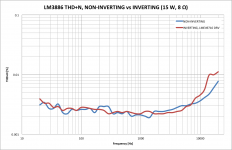
Inverting vs Non-Inverting THD
Just throwing a wrench in your works here. You're welcome, buddy... 🙂
🙂
I've been curious about inverting vs non-inverting as well. I understand the theory behind it. If the common-mode voltage varies (as it does in the non-inverting configuration), there is potential for the introduction of common-mode related distortion products. So I ran a THD sweep. See attached.
The circuit is the "GND STAR" topology I posted last night in the LM3886 PCB vs P2P Thread, Post #30. For the inverting configuration I added an LME49710 buffer to drive the 1 kΩ input impedance of the inverting LM3886.
Note that the noise floor of my HP 8903A results in a reading of 0.0018~0.002 % THD+N, so basically, the two circuits are neck and neck with the test equipment until about 5 kHz when the inverting configuration shows slightly worse THD. I plan to retake the measurement using an AP SYS-2712 that I just happen to have access to... 🙂 Stay tuned.
~Tom
Just throwing a wrench in your works here. You're welcome, buddy...
🙂I've been curious about inverting vs non-inverting as well. I understand the theory behind it. If the common-mode voltage varies (as it does in the non-inverting configuration), there is potential for the introduction of common-mode related distortion products. So I ran a THD sweep. See attached.
The circuit is the "GND STAR" topology I posted last night in the LM3886 PCB vs P2P Thread, Post #30. For the inverting configuration I added an LME49710 buffer to drive the 1 kΩ input impedance of the inverting LM3886.
Note that the noise floor of my HP 8903A results in a reading of 0.0018~0.002 % THD+N, so basically, the two circuits are neck and neck with the test equipment until about 5 kHz when the inverting configuration shows slightly worse THD. I plan to retake the measurement using an AP SYS-2712 that I just happen to have access to... 🙂 Stay tuned.
~Tom
Attachments
Last edited:
Input bias
Tom yer calculations don't account for normal input bias current , which creates an additional term
should be 3 terms Vos , Ios , Ib
normally Ib cancels out on good designs ( see data sheet test circuit )
The Ib term cancels out if the DC resistance "seen" by the non-inverting input and that "seen" by the inverting input are equal. At that point, you're left with the impact of the Ios term.
your assumption Rp= Ri//Rf assumes DC driven input (not the case here )
there is a DC block forcing all bias current through Rf.
You are correct, Sir. I missed the input coupling cap. I'm working on an LM3886 circuit that's DC coupled, so there was some interference going on in my brain.
In the case with the AC coupling on the input, you'll need R2 = R4.
For DC, the gain of the amp from the non-inverting input to the output is 1 V/V as C1 acts as an open circuit. The Ib from the inverting input flows through R4. This sets up Vout = -Ib*R4. For full Ib compensation, R2 needs to provide -Vout. So: R2*Ib = -(-Ib*R4) = Ib*R4 --> R2 = R4. That still leaves the Ios term, but that's (usually) small compared to Ib.
I don't know which "data sheet test circuit" you're referring to. I'm assuming the DC test circuit (Test Circuit #1, page 5). That circuit is designed to measure the DC parameters, not to provide the lowest Vos. Many times the DC test actually is set up to exacerbate the DC parameters so they can be measured fast with high precision. Test time is money. Big money...
~Tom
You are correct, Sir. I missed the input coupling cap. I'm working on an LM3886 circuit that's DC coupled, so there was some interference going on in my brain.
In the case with the AC coupling on the input, you'll need R2 = R4.
well thanks, I was beginning to wonder if my posts were invisible.
as I said post 29 there is a big mismatch between R2 and R4. with Ib bias is about 10 times Ios AND this resistor mismatch, this offset is huge, along with an unknown tempco factor.
The schem. in post 30 with my changes to Rb ~14K should be better all around. IMO
Also might consider at least doubling the input AC impedance to 2K.
yes the DC test circuit in the data sheet e.g. balanced 50 ohm inputs. > makes Vos dominate and very easy to measure with accuracy.
Last edited:
- Status
- Not open for further replies.
- Home
- Amplifiers
- Chip Amps
- Inverting LM3886