From the draft version of the manual, which should be up shortly:
The Teleporter is pretty simple to configure. There is one dip switch that determines if a channel is a LVDS receiver or a transmitter. The 4 switch positions are numbered 0 – 3.
When a switch position is open (off) the corresponding channel is a transmitter. A channel that is a transmitter will receive 3V LVCMOS signals on the SE header position marked with that channel and will output that signal as LVDS on the same channel at the diff/RJ45 connector.
When a switch position is closed (on) the corresponding channel is a receiver. A channel that is a receiver will receive LVDS on the same channel at the diff/RJ45 connector, and output 3V LVCMOS signals on the SE header position marked with that channel.
The PCB marks the polarity of the differential LVDS signals. The PCB also marks the SE channels on the header.
Just a small question, what is the consumption of the board? Thx
It will vary but it should be less than 150ma.
My pair of Teleporters are on their way from the USA. I'm now wondering how best to use them and my final objective (if there's any such thing in DIY Hi-Fi...) is to get my grubby hands on the anticipated TP USB module, have this close to my computer and use the Teleporter betwixt this and my Buffalo II.
Meanwhile, I was intending to utilise the Teralink USB/SPDIF convertor I currently use which has an I2S output via a CAT-type socket but I was wondering if there's a simpler, more effective way of going USB - Transporters -DAC?
Meanwhile, I was intending to utilise the Teralink USB/SPDIF convertor I currently use which has an I2S output via a CAT-type socket but I was wondering if there's a simpler, more effective way of going USB - Transporters -DAC?
Received today the Teleporters, as I understood:
150mA
+5-7,5V
PCM
0 - bit clock
1 - word clock
2 - data
3 - optional master clock (typically not used)
DSD
0 - bit clock
1 - data left
2 - data right
3 - (unused for asynchronous stereo - but coul dpossibly be master clock)
Attached pic, Left teleporter "off" is transmiter right Teleporter "on" is receiver? I have to connect 4 I2S wires and I have 8 holes, wich one have I to use (where is writed SE near the numbers: 0, 1, 2 & 3)?
Attachments
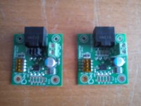
If you look closely, the holes further from the board edge are connected to the ground plane. Therefore, you want to use the four holes closest to the edge.
Are those jumpers on the LVDS header on the module on the left? If so remove them, you would never want to do that.
If you look closely, the holes further from the board edge are connected to the ground plane. Therefore, you want to use the four holes closest to the edge.
Thanks Brian
Are those jumpers on the LVDS header on the module on the left? If so remove them, you would never want to do that.
How can configure for receiver & transmiter?
That's what the switch is for - on the left of the board in your pictures.
The LVDS header is there to allow people to use their own RJ45 connector(wired) or direct wire the LVDS signal between two modules.
The LVDS header is there to allow people to use their own RJ45 connector(wired) or direct wire the LVDS signal between two modules.
Are those jumpers on the LVDS header on the module on the left? If so remove them, you would never want to do that.
This also shows the importance of having a manual for the Teleporter.

Sure I have a draft of it done, and Brian is just reviewing it before posting it.
If you are not confident wait for the manual before starting work.
If you are not confident wait for the manual before starting work.
That's what the switch is for - on the left of the board in your pictures.
The LVDS header is there to allow people to use their own RJ45 connector(wired) or direct wire the LVDS signal between two modules.
So I have the DIP switch all four positions "off" for the transmitter & all four positions "on" for the receiver, attached pic (where was jumpers now is the transmiter), it's OK?
Attachments

Yeah, thanks again Brian🙂
I have in mind to power separately both Teleporters, it's necessary a very good shunt regulatort or simply a LM317?
I have in mind to power separately both Teleporters, it's necessary a very good shunt regulatort or simply a LM317?
Last edited:
Yeah, thanks again Brian🙂
I have in mind to power separately both Teleporters, it's necessary a very good shunt regulatort or simply a LM317?
Teleporter has a local regulator, so you don't really need anything too fancy. Lm317 type is just fine. 🙂 Even LM7805 is fine.
The supply range on the Teleporter is pretty flexible. 4-8V should be perfectly fine.
:EDIT: 9V may be on the high side - looking at the VREG junction temp. I would recommend 4-6V if you can do it and about 8V max.
I will double check this when I get home later.
Last edited:

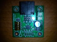
Attached Sidecar pic, I believe:
PCM
Teleporter receiver - Sidecar
bit clock - BCK
word clock - D1/LRCK
data - D2/DATA
DSD
bit clock - BCK
data left - D1/LRCK
data right - D2/DATA
It's OK
Yes that is the correct signal order for PCM and DSD.
Teleporter has a local regulator, so you don't really need anything too fancy. Lm317 type is just fine. 🙂 Even LM7805 is fine.
The supply range on the Teleporter is pretty flexible. 4-8V should be perfectly fine.
:EDIT: 9V may be on the high side - looking at the VREG junction temp. I would recommend 4-6V if you can do it and about 8V max.
I will double check this when I get home later.
Did you checked?
Yes that is the correct signal order for PCM and DSD.
Thank you
Yes 8V is as high as I would recommend. You might be able to get away with 9 or more but I wouldn't push it.
Thanks Russ, just connected the Teleporter with the BIII, now I have to start the most critical part: taking I2S from my CEC TL1 transport.
It's possible if using I2S avoid the dropouts due to connect separately the clock?
It's possible if using I2S avoid the dropouts due to connect separately the clock?
- Home
- More Vendors...
- Twisted Pear
- Introducing the bit "Teleporter"