Thanks Tom 🙂
Still need to ask the following questions. Sorry if some of these questions seem a little basic.
1. Can R2 and R3 be greater than 68R
2. What do you recommend as the maximum value for R14
3. How did you replace R1 with the 25K potentiometer (ie. insert it into the circuit)? Also, since you recommend that R1 should not be less than 2.2K and since a potentiometer can drop below 2.2K, is this a problem?
thanks
🙂
The values for the FET gate resistors are not critical. I used 68 ohms since I had a lot of them. I would not go above 100 ohms; but lower values are fine.
You can make R14 equal to R15, if you want a gain of 2 and it will be stable.
As far as changing the drain resistors on the first stage, it is possible, but it would require a significant redesign. The NFB is modest as is, and I have been pleased with the results. I am very happy with the sound too.
If someone does make that change, please post your results.
Thanks Tom 🙂
One more question (sorry about this)
- Where did you connect your volume pot wrto the circuit?
thanks
One more question (sorry about this)
- Where did you connect your volume pot wrto the circuit?
thanks
Two question to the designer
- The range of the Idss of the output jfet pairs to avoid forward biasing ??
- Don't you think it would be better to match also the input and second stage jfets with Vgs parameter to ensure DC stablility??
- The range of the Idss of the output jfet pairs to avoid forward biasing ??
- Don't you think it would be better to match also the input and second stage jfets with Vgs parameter to ensure DC stablility??
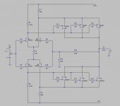
Here's where the input pot would go. Sorry I don't have a better schematic representation for a pot.
I set the input bias to approximately 3 mA with the values shown. The inputs will not be forward biased at that level. With a 330 ohm bias resistor, the input devices will be running at 50 to 60% of their idss which is very linear for them from their device curves.
Closer matching on the second stage devices may lower the DC offset a little, but there will be no stability issues.
Attachments
Thanks Tom
The circuit looks like it should be really quiet, especially the paralleled jfets in the output stage, which should have a very low output impedance (dependant on the cap) and be quiet linear due (I think) to local FB. Also less global NFB is needed. 🙂
Very nice and simple ... except for all the jfet matching ...
I would like to reduce the gain to 6 db, so I let you know what I come up with.
thanks 🙂
I have tried several different types of film/foil capacitors with good results. I am currently using a Bennic Metallized Polypropylene Capacitor and am happy with the results. I'd avoid aluminum electrolytics.
Hi Tom
I have been trying to OrCAD Pspice your circuit, but I have unable find the library component details for the Jfets ((ie. Pspice library component details for 2N5459, 2N5462).
Would you be able to help me with the library component file for these Jfets? or could someone else help?
thanks
I have been trying to OrCAD Pspice your circuit, but I have unable find the library component details for the Jfets ((ie. Pspice library component details for 2N5459, 2N5462).
Would you be able to help me with the library component file for these Jfets? or could someone else help?
thanks
i found these with google in just a few mins:
2N5459
http://www.seas.upenn.edu/~jan/spice/spice.models.html#JFETS
http://www.fairchildsemi.com/pf/2N/2N5459.html#models
http://www.duncanamps.com/spice/jfet/njfet.mod
2n5462
http://www.littlefishbicycles.com/poweramp/standard.jft http://www.ece.uci.edu/eceware/ads_docs/vcap/vcap113.html http://edocs.soco.agilent.com/display/ads2008/P-Channel+JFET+Models
however, regarding accuracy, use at your own risk ...
mlloyd1
jonusgrumby said:I'm sorry, I don't. Hopefully someone else will.
Thanks mlloyd1
New to Pspice ...
If I can ask another question of you
... how do you add the component details to the Pspice library.
thanks
New to Pspice ...
If I can ask another question of you
... how do you add the component details to the Pspice library.
thanks
jonusgrumby said:I have tried several different types of film/foil capacitors with good results. I am currently using a Bennic Metallized Polypropylene Capacitor and am happy with the results. I'd avoid aluminum electrolytics.
Thanks Tom
A question ... would it be easy to add a DC offset trim to remove the need for C1?
Of course, without affecting the circuits performance.
thanks
A friend of mine built one and varied R8 (slightly) to trim the DC offset. I think he used a 620 ohm resistor and a 200 ohm trim pot. He said it worked. I have never tried it, but it should work fine.
Originally posted by jonusgrumby A friend of mine built one and varied R8 (slightly) to trim the DC offset. I think he used a 620 ohm resistor and a 200 ohm trim pot. He said it worked. I have never tried it, but it should work fine.
Hi Tom
That's excellent, and that means that C1 is not necessary.
That also means that you have designed an excellent preamp.
Well done 🙂
Also, still teaching myself to use Pspice at the moment.
I will keep you informed ...
thanks

- Status
- Not open for further replies.
- Home
- Amplifiers
- Solid State
- Inexpensive JFET Preamp