Post 1.
The fix is in two parts.
1). I suggest a parallel pair of either 470u or 680u per each rail, directly at the chip. Forget the 100n bypass cap, since 470u||470u -OR- 680u||680u already has a bypass cap. Just get the electros as close to the chip as possible. Smaller caps will do louder midrange or larger caps is more laid back. Suggestion: Aim for clear baritone at loudness approximately level with the midrange. That won't happen; however, do try for clear bari. Suggestion: If you desire additional bypass cap, try 10n polyester.
2). Force the power decoupling to work with a series element. You can use either a custom made audiophile cable for umbilical between the 20,000uF per rail power board, cabled to, amplifier board -OR- my personal favorite is the simplicity of using a diode as a series element to force the decoupling to work. Per rail, that simple method looks like: BR, 20,000u, 10A1 Diode (or other series element), 680u||680u, LM3886.
Now, how does it sound with working power decoupling?
P.S.
The 680u||680u (or 3x470u) examples may be suitable for non-inverting LM3886. However, if you have a different, less nervous, chip like an STK or TDA7293, the same approach works, but a different chip could need smaller caps, like 220u||220u for amplifier board decoupling (and an appropriate series element to allow power decoupling to work).
There is decoupling shown, but it is disabled. Your amplifier board decoupling caps are effectively 20,050.100uF per each rail. That would be a great idea for the output section of a discrete amplifier. But it is a horrible idea for a small signal voltage amplifier. Both sections are enclosed in an LM3886 chip. Therefore dysfunctional power decoupling has distorted the small signal voltage amp inside. That's why you're having frequency response and harmonic distortion issues, no matter how hard you work on the stability compensation.Currently listening with LM3886 amplifier 20,000μF for each side in the psu. The sound is very detailed, and have dark sound signature. But the highs is not pleasant and the mids is laid back. In summary the sound not "live" as the great LM1875. Are there any recommendations how to improve the LM3886?
Schematic of amplifier: http://www.interload.co.il/upload/6365504.bmp
The fix is in two parts.
1). I suggest a parallel pair of either 470u or 680u per each rail, directly at the chip. Forget the 100n bypass cap, since 470u||470u -OR- 680u||680u already has a bypass cap. Just get the electros as close to the chip as possible. Smaller caps will do louder midrange or larger caps is more laid back. Suggestion: Aim for clear baritone at loudness approximately level with the midrange. That won't happen; however, do try for clear bari. Suggestion: If you desire additional bypass cap, try 10n polyester.
2). Force the power decoupling to work with a series element. You can use either a custom made audiophile cable for umbilical between the 20,000uF per rail power board, cabled to, amplifier board -OR- my personal favorite is the simplicity of using a diode as a series element to force the decoupling to work. Per rail, that simple method looks like: BR, 20,000u, 10A1 Diode (or other series element), 680u||680u, LM3886.
Now, how does it sound with working power decoupling?
P.S.
The 680u||680u (or 3x470u) examples may be suitable for non-inverting LM3886. However, if you have a different, less nervous, chip like an STK or TDA7293, the same approach works, but a different chip could need smaller caps, like 220u||220u for amplifier board decoupling (and an appropriate series element to allow power decoupling to work).
Last edited:
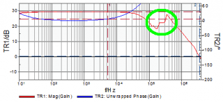
See my simulation results below.
Here are some real results -- you won't get this from the model:
Uncompensated:
An externally hosted image should be here but it was not working when we last tested it.
Compensated 22K+47pF:
An externally hosted image should be here but it was not working when we last tested it.
The amp above is not compound with the OPA2604 as Bob had shown, and it does have an output zobel.
This is prettier -- use 9.1k as the shelving resistor:
An externally hosted image should be here but it was not working when we last tested it.
Those look like closed loop plots. Open loop is more interesting for stability. If you have the op-amp/LM3886 running as an inverting amp, you can measure the loop gain at the inverting input pin. What you'll measure is actually the residual error voltage, but that is inversely proportional to the loop gain, so all you have to do is change the sign on the magnitude curve (in dB) to get the loop gain.
That said, the peaking shown in the uncompensated case may be indicative of marginal stability. OTOT, the "wonkiness" at 100-400 kHz in the compensated case is a bit disturbing. Is that a measurement issue?
Thanks for sharing! I do plan to take those loop gain measurements myself "one of these days". Hopefully before too long.
One question: What was the load impedance for above measurements?
~Tom
I don't think it's a measurement issue as I calibrated the probes before doing the runs.That said, the peaking shown in the uncompensated case may be indicative of marginal stability. OTOT, the "wonkiness" at 100-400 kHz in the compensated case is a bit disturbing. Is that a measurement issue?
Hi Jackinnj those are some great graphs. What was the setup that you used to measure the gain and phase curves? Was it a manual or automated process?
Hi Jackinnj those are some great graphs. What was the setup that you used to measure the gain and phase curves? Was it a manual or automated process?
You can do much the same with an inexpensive sweep generator and a "new-ish" oscilloscope (they plot phase). I also bought an HP3577A when the tech bubble burst 10 years ago but it isn't very happy with high voltages.
The HP3562A can measure gain/phase. Unfortunately, only to 100 kHz. Last time I measured loop gain, I used a network analyzer...
~Tom
~Tom
I've just placed an order for a Velleman PCSGU250 USB Scope + Function Generator. At $145 (from Amazon) this is appears to be the cheapest device for creating Bode and FFT plots.
0.005Hz to 500kHz Function Gen.
10Hz -500kHz Bode plot
12MHz spectrum analyzer
2048 lines FFT resolution
0.005Hz to 500kHz Function Gen.
10Hz -500kHz Bode plot
12MHz spectrum analyzer
2048 lines FFT resolution
I don't think it's a measurement issue as I calibrated the probes before doing the runs.
Calibrated or not, the abrupt changes in gain and phase don't look real. It could be that not enough points were used in the sweep or the interpolation between points screw things up.
Also, you're looking at the closed loop gain rather than the open loop or loop gain. While the closed loop gain is interesting, what you want to look at for a stability analysis is really the loop gain.
If you have the HP3577, I suggest taking a look at HP/Agilent's app note for how to make the loop gain measurement: HP3577A Loop Gain Measurements. You can always use a voltage divider to reduce the voltage applied to the HP3577 inputs. Just remember to factor this into the loop gain. I think that model has a 1 MOhm input impedance mode so you can use regular 10x oscilloscope probes. That would work around the high voltage issue as well.
~Tom
Last edited:
Same for me, now that I have a network analyzer (W&G SNA-2). Health and workload issues contantly get in the way of DIY activities these days (*sigh*).I do plan to take those loop gain measurements myself "one of these days". Hopefully before too long.
The plots were done with the LM3886 in non-inverting mode, the conventional amplifier gain of 26dB, without benefit of Cordell's inverter and buffer. The dashed plot is "memory". Yes, I understand that I should break the loop between the buffer and the inverting input.
Would probably be a good idea to measure the open-loop gain of the LM3886 to confirm what's in the data sheet.
An externally hosted image should be here but it was not working when we last tested it.
Would probably be a good idea to measure the open-loop gain of the LM3886 to confirm what's in the data sheet.
Hi, I have some questions. Are the abrupt changes in gain and phase we can see in jackinnj plots the result of parasitics caused by the PCB and parts? I was able to get some really ugly sim-plots by adding small caps and coils in the feedback network. (Playing with the rails had no effect yet)
How can we test these parasitics best?
How can we test these parasitics best?
I am not aware of any analog system that can create an abrupt change in amplitude or phase. There's always a smooth transition. It could be that the amplitude/phase responses do change smoothly, but there aren't enough data points to determine that.
~Tom
~Tom
I am not aware of any analog system that can create an abrupt change in amplitude or phase. There's always a smooth transition. It could be that the amplitude/phase responses do change smoothly, but there aren't enough data points to determine that.
~Tom
What abrupt change in gain are you describing? The compensated LM3886 in post 103 seems to have a pretty normal slope. The dashed line is the data in memory, and it shows a pretty dramatic impedance change which you won't find in the TI model.
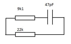
Solid curve of plot #2 (22k+47pF) is dashed curve of plot #3 (9k1).
That ragged irregular rise of some 15dB magically disapears when just a single resistor is changed? (exact schematic would be nice, it's unclear how you've set the gain exactly). Looks definitely unreal to me, especially from the "sawtooth" blip which is still present in the second curve. Further, the 0dB crossing is not at the same frequency but two ocatves lower (1MHz vs 4) which looks like a very clear indication to me something went wrong in the measurement scaling/normalization.
That ragged irregular rise of some 15dB magically disapears when just a single resistor is changed? (exact schematic would be nice, it's unclear how you've set the gain exactly). Looks definitely unreal to me, especially from the "sawtooth" blip which is still present in the second curve. Further, the 0dB crossing is not at the same frequency but two ocatves lower (1MHz vs 4) which looks like a very clear indication to me something went wrong in the measurement scaling/normalization.
Solid curve of plot #2 (22k+47pF) is dashed curve of plot #3 (9k1).
That ragged irregular rise of some 15dB magically disapears when just a single resistor is changed? (exact schematic would be nice, it's unclear how you've set the gain exactly). Looks definitely unreal to me, especially from the "sawtooth" blip which is still present in the second curve. Further, the 0dB crossing is not at the same frequency but two ocatves lower (1MHz vs 4) which looks like a very clear indication to me something went wrong in the measurement scaling/normalization.
He means 22k\\(9k1+47pF).
Attachments
What abrupt change in gain are you describing?
See attached. Sorry for the belated response. I'm working on getting my own loop gain/phase measurements going.
~Tom
Attachments
See attached. Sorry for the belated response. I'm working on getting my own loop gain/phase measurements going.
~Tom
Tom -- that's the uncompensated LM3886 -- with the Zobel on the output.
- Status
- Not open for further replies.
- Home
- Amplifiers
- Chip Amps
- Improving the LM3886 amplifier