Klaus posted an outline schematic a few years back, but that's only one way to accomplish it. In essence its necessary to reference signal ground to VEE and ensure that load currents don't modulate this voltage. Having just one set of caps, between VCC and VEE and AC coupling the load to VEE works, another method is to run bridged (two amps in antiphase).
It sounds like using a single supply and AC coupling the output would work. Then you just move the problem to the output cap... 🙂
You could also do what I did and design an amplifier that uses the LM3886 but has stellar supply rejection thanks to an error-correction loop. I'm getting down below 0.0004 % THD (1 kHz, 22 kHz BW) just before clipping using a real supply. My circuit performs just as well on a real supply as it does on a lab supply. Only with a lab supply you get a few more watt of output power as the supply sag is eliminated with the regulated supply.
~Tom
Looking at the equivalent circuit schematic in the LM3886 data sheet, it becomes pretty obvious why the VEE PSRR is so much worse than the VCC. The VAS sits on VEE... I would have been nice if the amp had been differential all the way to the output stage.
~Tom
~Tom
I have swapped between AGND and PGND on other designs, and confirm that connecting to PGND provides slightly better detail on the LM3886.Pin 7 (GND) can connect to AGND or PGND. Personally, I would connect it to PGND to keep AGND clean. The quality of the "ground" at the GND pin only affects circuit performance in mute. I'm not so concerned about the sound quality when the amplifier is muted... 😛
...
~Tom
For a desktop computer speaker application, I'd probably opt for one of the buffer ICs such as the LME49600. I suspect one is probably sufficient to drive a speaker to a reasonably loud volume. Put a few in parallel if you want more oomph.
Maybe I'm misunderstanding your "T-net" thing. I'm thinking of the topology commonly used to create a high gain circuit or to lower the impedances in the feedback network to combat issues related to high op-amp input capacitance. That circuit is a T-network from the op-amp output to the op-amp input forming the feedback. It's basically like the regular resistive feedback network with a voltage divider before the feedback resistor. Is that what you're referring to?
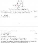
Fig. 3.10 in this .pdf is what I'm talking about. That circuit, if used with an LM3886, does nothing to address stability issues related to gains below 10 V/V. The loop gain/phase is the same with the T-network as it would be with the regular feedback network. The only advantage of the T-network is that it reduces the impedances in the feedback network. This may help in high-gain situations where the input capacitance of the op-amp along with the high resistance feedback resistor would cause a pole in the feedback transfer function, dorking up stability.
If Andrew wants PM > 80 deg at gains below 20 V/V, he'll need to apply phase lead/lag compensation to the LM3886. No T-network will work around that fact.
~Tom
I think he was referring to Thorsten Unity Chipamp. If I understand your point, it shouldn't work. I've always wanted to throw it together ...
Ah, the trick is, it has to be inverting and the 'T' is config'd differently!
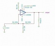
Here's T's circuit description:
"...you can extremely easily get unity gain in inverting mode. Simply use a pair of 220k Resistors, one from the Amp input to the inverting input, the other from the inverting input to the Output.
NOW observe the magic. Place a 22k resistor between the inverting input and ground. Then place an 18k resistor between the positive input and ground. Unity gain and stable. Easy as pie.
Sayonara
PS, this same sort trick lets you use the OPA637 as I/V converter without osccillation. It sounds notably better than OPA627 in this position but is not unity gain stable.... "
from
http://www.diyaudio.com/forums/chip-amps/9852-gainclone-no-gain-yes-pain.html#post112061
Here's what it looks like:
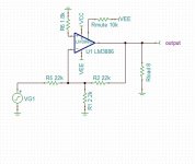
But I prefer the low res one (just div all res by 10):
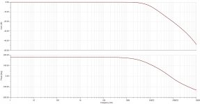
😎
Here's T's circuit description:
"...you can extremely easily get unity gain in inverting mode. Simply use a pair of 220k Resistors, one from the Amp input to the inverting input, the other from the inverting input to the Output.
NOW observe the magic. Place a 22k resistor between the inverting input and ground. Then place an 18k resistor between the positive input and ground. Unity gain and stable. Easy as pie.
Sayonara
PS, this same sort trick lets you use the OPA637 as I/V converter without osccillation. It sounds notably better than OPA627 in this position but is not unity gain stable.... "
from
http://www.diyaudio.com/forums/chip-amps/9852-gainclone-no-gain-yes-pain.html#post112061
Here's what it looks like:

But I prefer the low res one (just div all res by 10):


😎
Last edited:
What are the disadvantages of using this High Noise Gain arrangement compared to normal gain arrangements?
What stability margins exist for the high noise gain arrangement?
Are they the same as using the chip at a real gain of 10times?
What stability margins exist for the high noise gain arrangement?
Are they the same as using the chip at a real gain of 10times?
The noise gain's the same as for the standard (20 or 26dB gain) arrangement, just the signal gain is reduced.
What are the disadvantages of using this High Noise Gain arrangement compared to normal gain arrangements?
What stability margins exist for the high noise gain arrangement?
Are they the same as using the chip at a real gain of 10times?
I just reinstalled Ti's TINA and have tomchr's clever 3886 loopstability file:
http://www.neurochrome.com/audio/wp-content/uploads/2014/02/LM3886-LoopStability.TSC_.txt
from his awesome:
LM3886 Chip Amp Stability Analysis
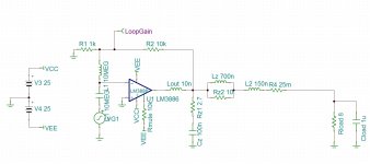
I'll see if I can figure out how to run the sims ...

What are the disadvantages of using this High Noise Gain arrangement compared to normal gain arrangements?
What stability margins exist for the high noise gain arrangement?
Are they the same as using the chip at a real gain of 10times?
From the linked old thread:
http://www.diyaudio.com/forums/chip-amps/9852-gainclone-no-gain-yes-pain.html
"
...
Hi,
If i may volunteer a reply the 22k resistor is there to provide stable dc reference.
T: Wrong. It's there to provide a noise gain of slightly over 10, ensuring the amp is stable.
Sayonara
...
jan.didden:
Sayonara,
You are right on target of course. May I suggest, in the interest of lower noise, to divide all resistor values by 5 or 10?
Jan Didden
...
phase_accurate:
JAZZ' idea of a voltage divider may not be as silly as it sounds from a first view.
If you make this happening only at high frequencies, where also the oscillation usually takes place (BTW: has anybody an idea about the frequency range ?), then you won't affect audible noise and you have an additional input slew-rate/RF pickup reduction.
I don't have any of these ICs on hand but if someone is experimenting with these anyway it won't take much time to try it out.
One simply splits the input resistor in two different sized parts, for instance with a ratio of 1:3. The smaller one being closer to the inverting input. From the node between the two resistors you connect a capacitor to ground forming a lowpass with
fc=1/(2*Pi*C* R1a//R1b).
The upper cutoff frequency should be chosen well out of the audio range.
Just my two pence.
Regards
Charles
...
Hi, But, what is the role of 22k resistor?
T: To make the Amp think it has a gain of 10 and thus to stop oscillating.
...
...
Hi, Yes you can: resistor from output to -input = 0 ohm, resistor between - input and ground = infinite...
T: Not with an LM3875 or LM3886. They will be instable at such a low gain. Sorry kid, no dice...
Sayonara
...
mc2:
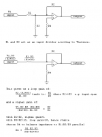
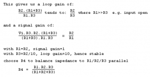
"There seems to be a deal of confusion over this circuit configuration.
In fact this is a conventional technique for getting a signal gain less than the minimum stable loop gain with an op-amp.
I have expanded the math in the attached diagram. In essence the configuration provides an above unity loop gain (in this case approx. 11) but at the same time attenuates the input signal in exactly the same proportion, hence preserving the signal gain.
You can see this effect in the way the effect of R3 cancels out in the signal gain equation below.
mc2 "
😎
😎
...
gootee :
But it doesn't sound like the lower gain is a viable option, in his case, unless he can live with a fraction of a watt of output. Or am I missing something?
abraxalito:
spindre17 is saying he can live with such low output levels. But then again, at such low levels the noise of your suggested approach is likely to be inaudible too
And wouldn't the source's noise also be attenuated by the divider? If so, then where does the greater noise come from?
abraxalito:
It appears a chipamp's noise is generally limited by its input. The schematics I've looked at show heavily degenerated LTPs (using 3k3 resistors in LM1875's case) as a first stage which tend to mean much higher noise than opamps. So higher signal levels at the input mean lower output noise in general. Attenuating then gaining up will amplify the input noise much more than running at lower gain.
...
from:
http://www.diyaudio.com/forums/chip-amps/9852-gainclone-no-gain-yes-pain.html
Last edited:
Are you saying that the only disadvantage is higher noise levels?
or am I reading too much into the extracts you have posted?
I have the view that using a 3886 @ a normal gain of 10times leaves us with stability margins that are too low for good performance or good sound quality.
I prefer using a gain of around 26times to 30times to get the benefits of the improved stability margins at that gain.
Being mindfull of my opinion, I ask again
What stability margins exist for the high noise gain arrangement?
Are they the same as using the chip at a real gain of 10times?
First I need to apologize for the mistake, my final decision was AGND or signal ground.I have swapped between AGND and PGND on other designs, and confirm that connecting to PGND provides slightly better detail on the LM3886.
Next I discovered somthing interesting during a simulation. The GND on the LM3886 chip seems to provide an interesting compensation. When one can use is along with ground layout to change the power going through speaker loads. If you have a dip in power around Fo, you can use that pin to flatten out the power dip. Tried it, and a big difference...
Speaker ground at RCA jack or potentiometer gives the biggest imaging/soundstage with the least practical tone and worst stability. Speaker ground at amplifier board gives the middle ground but would require big decoupling capacitance to preserve stability and provide a practical tone for use. Speaker ground at power supply gives the least imaging/soundstage with the most friendly tone and highest stability.
It is linear.
That is uninteresting, because it is probably more fun to work at some other area well before having to make those choices.
It is linear.
That is uninteresting, because it is probably more fun to work at some other area well before having to make those choices.
I think grounding is definitely an interesting issue because I have found it does influence sound in many ways, but it seems an RCA input ground is normally connected to the same power ground as the speaker return. But the pin7 on the LM3886 really deserves more attention.
But the pin7 on the LM3886 really deserves more attention
Why? As TomChr points out, it's only used for the mute function, unless you're concerned about sound quality when muted. 😉
Mike
If you think the available data presents the whole story, you can hang you hat on that. I am only sharing from actual experimenting with different application, but I would suggest you do some simulation and experimenting on your own to find a good way to use it. I could show some simulations, but it would be best for each to convince yourselves. Remember TomChr was asking for speaker driver load examples? Than means he wants to see how real loading effects the amplifier. I think that is a good indication for more advanced designs.
My view is "You never learn anything new if you go by the book." I like to reasonably explore options and find out what works, then figure out why to get consistent results.
My view is "You never learn anything new if you go by the book." I like to reasonably explore options and find out what works, then figure out why to get consistent results.
Last edited:
As far as Grounding pin 7, yes.If you think the available data presents the whole story
Been there, done that, never measured nor heard any difference.but I would suggest you do some simulation and experimenting on your own to find a good way to use it
I'm not sure how any of that applies to the "grounding pin 7" issue (or in my teeny mind, non-issue.)Remember TomChr was asking for speaker driver load examples? Than means he wants to see how real loading effects the amplifier. I think that is a good indication for more advanced designs.
So I'm still wondering why you think "the pin7 on the LM3886 really deserves more attention."
Mike
OK, I'm confused (Or maybe just stupid?) Are you connecting pin 7 to something other than ground?
Mike
Mike
- Status
- Not open for further replies.
- Home
- Amplifiers
- Chip Amps
- Improving the LM3886 amplifier