Looking back at the original schematic, I realise I made a mistake.It can't be Cgs, for that the output has to have the lower voltage.But here the driver side is the lower one, so the clipping is not in the mosfet's but the driver BJT's.
Mona
Mona
call to order
Gentlemen, reflections here are pretty useless without knowing the frequency in question (picture of post 1).
Gentlemen, reflections here are pretty useless without knowing the frequency in question (picture of post 1).
thanks for all the replys.
i will give this a try when i get a chance.
i know the circuit is still stable with lower values of R12/13, so i will try out 150/100R with the diodes, as this mod is easy to try out.
i will give this a try when i get a chance.
Try a reverse-biased diode in parallel with the gate resistors (R12, 13), it will allow the gate charge to be sucked out faster.
i know the circuit is still stable with lower values of R12/13, so i will try out 150/100R with the diodes, as this mod is easy to try out.
Gentlemen, reflections here are pretty useless without knowing the frequency in question (picture of post 1).
thats a 10KHz sine, at lower frequencies (3KHz) there is still some latchup effects, but no as much as at 10KHz. I think at 1KHz the clipping performance is acceptable...
( scope is set to 10v per div )
Last edited:
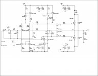
The power fets are Both shown as N types. Is this correct ?
well spotted, but one is p, and one is n, as shown by the part numbers.
Not related to the question but an observation. Shouldn't the power rails be the other way round. The MOSFETs with the lower voltage and the input stage the higher?
Paul
The transformer i am using is a 40v, giving rails of around 58v. With hindsight a 35v transformer would be more suitable, giving less dissipation in the output devices as it has been pointed out, however i am stuck with the 40v transformer.
However it does enable me to power the input/driver stages via a regulator circuit which i have set to 48v or so.
thats a 10KHz sine, at lower frequencies (3KHz) there is still some latchup effects, but no as much as at 10KHz. I think at 1KHz the clipping performance is acceptable...
( scope is set to 10v per div )
Thank you for this clarification. The clipping behaviour is frequency dependent.
What you see in screen picture of post 1 is perfectly acceptable and is all you
can expect from an amplifier topology like this, being about 40 years old. You
may want to add a shot of the voltage made at gate drive point under the same
conditions for comparison, preferably both on the same screen pic taken with
compensated probes.
Last edited:
The transformer i am using is a 40v, giving rails of around 58v. With hindsight a 35v transformer would be more suitable, giving less dissipation in the output devices as it has been pointed out, however i am stuck with the 40v transformer.
However it does enable me to power the input/driver stages via a regulator circuit which i have set to 48v or so.
You could run the IPS from higher rails by adding a small transformer with 15V dual secondary windings and stack these on top of the OPS transformer (40V) windings. You could then regulate down a little from there.
Or a cheaper method would be to add another couple of secondary windings to your current transformer.
Paul
I have exactly the same problem with clipping quality at the lower rail on a similar bipolar design I posted about maybe a week ago. Might be the nature of the beast?
Voltage doublers can be a good option for high voltage IPS and driver rails for FET based amps. Follow the doubler with a regulator for best performance.
if the original questioner wants to try a baker clamp schematic as used in a successful product, find the schematic of the APT 1 power amp and look at the VAS stage.
the schematic is posted on this site in a few places.
mlloyd1
the schematic is posted on this site in a few places.
mlloyd1
Did you allready tried it like this ?no luck with diodes across R12/13.....i think i will leave things as they are...
Mona
Attachments
hi,
I put two 1n4148 diodes in series with Q9's base and one from Q9's base to collector
your configuration for Q9 is different with only one diode in the base....
can you explain why you show diodes for Q8
Yes but also not the diode from base to collector but from diode before base to collector.
Your picture of the clipping shows something wrong at both peeks.One from Q9 and the other probably from saturation of Q8.
Mona
Your picture of the clipping shows something wrong at both peeks.One from Q9 and the other probably from saturation of Q8.
Mona
i have the same clipping trace at Q9 collector...
if I run the whole amp from +/- 30v rails I still have the same trace...
if I run the whole amp from +/- 30v rails I still have the same trace...
As said before what you see in screen picture of post 1 (10 kHz)
is perfectly acceptable and is all you can expect from an amplifier
topology like this. The relatively short overhang delay time seen
corresponds to a frequency of 500 kHz or so. Situation will not
change if you put diodes at random points of the schematic or
play with supply voltages.
is perfectly acceptable and is all you can expect from an amplifier
topology like this. The relatively short overhang delay time seen
corresponds to a frequency of 500 kHz or so. Situation will not
change if you put diodes at random points of the schematic or
play with supply voltages.
- Status
- Not open for further replies.
- Home
- Amplifiers
- Solid State
- implimenting a baker clamp