Hi Bensen, I glanced at the spreadsheet, will look at it deeper later, thanks for sharing it.
Say 7 is the right number for your situation, then definitely look into the potential problems I described earlier. 7 pairs is not easy to drive.
- At the base of the NPN, you have 7x250pF of cap + trace capacitance. That is is easily 1.8nF total and we are going with typical numbers in the datasheet, so it could be much worse, 2nf or more would not be surprising.
- For the PNP, Cob is 2x the NPN, so you have 7x500pF typ. + trace capacitance. Here you can easily have 3.5nF - 4nF of capcitance or more depending on how tight is Sankens manufacturing process.
Therefore, getting those nodes (output device bases) to move takes a lot of current due to i=Cdv/dt. Anyway, let us know what you see.
Datasheet links here for everyone to see:
https://www.semicon.sanken-ele.co.jp/sk_content/2sc3519_ds_en.pdf
https://www.semicon.sanken-ele.co.jp/sk_content/2sa1386_ds_en.pdf
sandrohv:
but isn't that input capacitance diminished by the bootstrapping action of the emitter follower configuration?
so, each device is only presenting a fraction of that max capacitance given in the datasheet.
mlloyd1
but isn't that input capacitance diminished by the bootstrapping action of the emitter follower configuration?
so, each device is only presenting a fraction of that max capacitance given in the datasheet.
mlloyd1
Hi Mlloyd, Cob is mostly base to collector cap, Cbe. Hence it is node to signal ground.
If you want to be mega exact, COBO = Ccb + Cce*Cbe/(Cce+Cbe). But Cce is really small, so I usually ignore it.
transistors - How are C(OBO) and C(IBO) defined? - Electrical Engineering Stack Exchange
Best, Sandro
If you want to be mega exact, COBO = Ccb + Cce*Cbe/(Cce+Cbe). But Cce is really small, so I usually ignore it.
transistors - How are C(OBO) and C(IBO) defined? - Electrical Engineering Stack Exchange
Best, Sandro
Last edited:
once an emitter resistor is installed, that swamps the other factors.
VBE - 50 to 100mV difference between any silicon transistor of similar current ratings
it is a function of the P-N junction.
Hfe - lowers the drive current.
a 0.33 ohm emitter resistor will easily balance every output device to within 1% at high power and 5% at low output power.
At low dissapation, it doesn't matter if one device is slightly different then the next.
oops , missed the "ob".
ok!
mlloyd1
ok!
mlloyd1
Hi Mlloyd, Cob is base to collector. Hence it is node to signal ground.
Best, Sandro
Hi stocktrader, everything you said is right except "5% at low output power".
It depends on what you mean with 'low output power' and what is your initial VBE mismatch.
Say IE=10mA per device and the RE=0.33ohms. Then RE*IC = 3.3mV which is << KT/q = 26mV. For RE to do something, you need at least VRE to be at least KT/q which translates to a power level where each transistor is running at ~IE=80mA per device (RE=0.33).
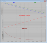
Look at the attached plot and setup. Devices were mismatched with 18mV of Delta VBE on purpose, hence ratio of 2x. REs are matched at 0.22 each. Therefore, at high current, the devices should run at a ratio of 1. X-axis is overall output current, top pane are IE, second pane is average VRE and third pane is ration between currents.
It takes a few KT/q of VRE for RE to do its job.
It depends on what you mean with 'low output power' and what is your initial VBE mismatch.
Say IE=10mA per device and the RE=0.33ohms. Then RE*IC = 3.3mV which is << KT/q = 26mV. For RE to do something, you need at least VRE to be at least KT/q which translates to a power level where each transistor is running at ~IE=80mA per device (RE=0.33).
Look at the attached plot and setup. Devices were mismatched with 18mV of Delta VBE on purpose, hence ratio of 2x. REs are matched at 0.22 each. Therefore, at high current, the devices should run at a ratio of 1. X-axis is overall output current, top pane are IE, second pane is average VRE and third pane is ration between currents.
It takes a few KT/q of VRE for RE to do its job.
Attachments
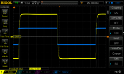
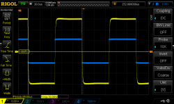
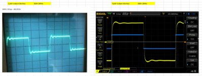
10Khz square wave tests in R//C load
Load is 8R with parallel following film caps: 10n, 100n, 0µ39, 0µ82, 2µ2.
Load is connected via a 2x2.5mm², 4m long speaker cable.
Measurements have been taken at negative feedback point on PCB. (before the L//R network)
Measurements have been done on circuit: https://www.diyaudio.com/forums/sol...ransistors-class-tou-match-6.html#post6164404
Please find scope screenshots below.
There is some small ringing visible on 0µ82 + 2µ2. But nothing to worry about, not?
Attachments


Last edited:
Hi Bensen, indeed.
I was hoping to see internal ringing, or something funny.
The oscillation you see is major loop instability due to capacitive load... expected behavior given your circuit... nothing to worry about in my opinion.
Going back a few posts back, please confirm that this is the overall problem you are trying to solve: "With the 7 pairs installed some detail was clearly gone, that's why I'm pulling my hair now if my matching afterwards was doen good enough. I'm assembling my second monoblock now, I only will add 1 pair of output devices in order to make a comparison between 1 pair and my 7 "matched" pairs of bjt's"
Problem: 7 pairs caused detail to be lost.
Hypothesis 1: Is matching the problem? Sandro says no.
Hypothesis 2: Is oscillation due to loading the problem? Does not seem the case given scope photos, but I would still put a probe on the base of each output device to see oscillations. Also, zoom in to the waveform right after the edge to see if you see a small oscillation there.
Finally, what does loss of detail mean? Increased distortion, degradation of frequency response? Can you provide something that can be quantified? That would help me a lot.
Best, Sandro
Thanks for the feedback, I'm rather happy you have the same opinion about the square wave reponse.
I just remembered I had some pictures of square wave tests done some time ago, but only with 1 pair of output devices (same circuit but different PCB).
Now we can compare the square waves done at 10kHz with a 8R//820n load.
With only 1 pair, the square wave respons is about identical, same damping but amplitude with 1 pair looks a bit bigger.
I can't quantify what I'm hearing. I have to wait until I can power up the second monoblock (I'm waiting on some copper/silver 11AWG wire for the power supply wiring), should arrive in a couple of days.
Attachments
Last edited:
Thanks to Sandroh for his excellent description and sims, this is my take on matching and those sims. Since most outputs are voltage driven its Vbe that should be matched, and thats what Re does, but I dont believe its necessary. People seem to confuse bias matching with running current. matching only matters at higher power. If your amps putting out 1 watt does it matter if most of it comes from one pair of outputs? Let the current increases to 1 ampin the first transistor, its Re sees 2.2v. If the vbe mismatch is 50mv the second Er sees 2.15v and 2.15/2.2 amps, pretty close. Go to 5 amps, where you realy need matching and the currents are even better matched. Than beta droop kicks in and the currents become even closer. If your still worried about one of the transitors drawing too much current, add apair.
Thanks cbdd, you are absolutely correct. Your math is off by 10x, but the point is correct (1Amp on 0.22ohms is 220mV not 2.2V 🙂 )
But yes, once V_RE is greater than Delta_VBE, the latter does not matter.
Not that it matters for this discussion, but in op-amp planet, since currents are smaller, RE is indeed in the order 2 to 5 ohms.
But yes, once V_RE is greater than Delta_VBE, the latter does not matter.
Not that it matters for this discussion, but in op-amp planet, since currents are smaller, RE is indeed in the order 2 to 5 ohms.
Last edited:
Thanks for the feedback, I'm rather happy you have the same opinion about the square wave reponse.
I just remembered I had some pictures of square wave tests done some time ago, but only with 1 pair of output devices (same circuit but different PCB).
Now we can compare the square waves done at 10kHz with a 8R//820n load.
With only 1 pair, the square wave respons is about identical, same damping but amplitude with 1 pair looks a bit bigger.
I can't quantify what I'm hearing. I have to wait until I can power up the second monoblock (I'm waiting on some copper/silver 11AWG wire for the power supply wiring), should arrive in a couple of days.
Great!
Benson, those large FET's you have driving the outputs have high input capacitance and large positive temp coefficients at the current (130ma) you are driving them at.
Does the idle current stay around 100ma when hot?
just got a batch of 2SC5200 , 2SA1945 to try with IRF610, 9610 drivers.
Does the idle current stay around 100ma when hot?
just got a batch of 2SC5200 , 2SA1945 to try with IRF610, 9610 drivers.
Benson, those large FET's you have driving the outputs have high input capacitance and large positive temp coefficients at the current (130ma) you are driving them at.
Does the idle current stay around 100ma when hot?
just got a batch of 2SC5200 , 2SA1945 to try with IRF610, 9610 drivers.
I’ve tried lot’s of bias spreaders, the one used with both a pnp and npn works super. With the resistor (10ohm in my case) between the emitters you can adjust very fine the temperature coëfficiënt. I slightly overcompensated. The bias in the output stage does not drop more than 5ma between cold and bloody hot (60C).
The idea of this bias spreader I have from the Parasound circuits. The JC1 uses the same fet’s as driver, but this is a coincidence.
Please explain the link between current and input capacitance? Would make 50 vs 130ma a big difference in these kind of high power fet’s?
The input capacitance affects the speed at which the VAS can drive them. My thinking is a smaller FET is both easier to bias and faster in the same position.
looks like your dual transistor spreader works perfect.
looks like your dual transistor spreader works perfect.
Ok, yes that I understand. Therefore I run my VAS at about 25...30mA.
Speed is no problem, have a look at the square waves, pretty good in my opinion.
And yes, I can highly recommend this bias spreader in combination with this topology. The fet’s have rather high Vgs compared to the Vbe of a bjt. With a single bias spreader device your multiplication factor between upper and lower resistor becomes to big... which results in rather big overcompensation.
Sandrohv , on Benson's amplifier he is driving 7 output pairs. Is there any difference in distortion if there is current mismatch between the pairs when driven at 1 watt output or less?
eg. 100ma first pair 68ma second 106 third ... etc.
eg. 100ma first pair 68ma second 106 third ... etc.
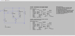
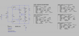
Probably not. Here is a quick experiment.
Setup:
- 2 pair output stage optimally biased
- Rload = 8 ohms
Experiment:
- Sweep VIN from -4V to 4V (1W RMS)
- Mismatch VBE by 0mV (perfect match) and 18mV
- Look at the wingspread diagram
From the simulation, you can see the variation in the wingspread diagram with a horrific mismatch is neglible, so I would expect minimal distortion difference. I think the reason is because IC1+IC2 is constant.
Actually, if you think about it, output transistors nowadays are composed of many small transistors inside the package (for speed and power dissipation). Who said current distributes evenly across these? I can bet it does not.
Attachments
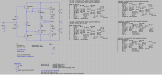
I also run a distortion analysis which agrees with my previous post.
Setup:
- Amplitude = 4Vp
- RLoad = 8ohms
Results:
+ Freq 1K
- No mismatch: 0.020482%
- With mismatch: 0.020245%
+ Freq 10k
- No mismatch: 0.021839%
- With mismatch: 0.022528%
+ Freq 20k
- No mismatch: 0.019886%
- With mismatch: 0.020246%
Bottomline, at 1WRMS, mismatch between devices seems to do little to distortion as long as optimum bias is applied to the array as a whole.
What about high power?
At 100W => amplitude of 40Vp with Rload = 8ohms
Results:
+ Freq 1K
- No mismatch: 0.044693%
- With mismatch: 0.044160%
+ Freq 10k
- No mismatch: 0.050742%
- With mismatch: 0.050469%
+ Freq 20k
- No mismatch: 0.058711%
- With mismatch: 0.058237%
It looks like at the other power level extreme, 100W, VBE match does not seem to matter either for distortion. I am not surprised since at high power levels VBE does not matter, it is RE what matters.
The screenshot is the setup.
Best, Sandro
Attachments
- Home
- Amplifiers
- Solid State
- If you put new output transistors, class A/B, will tou match them?