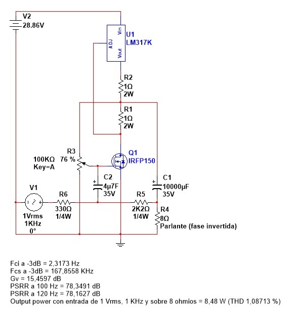
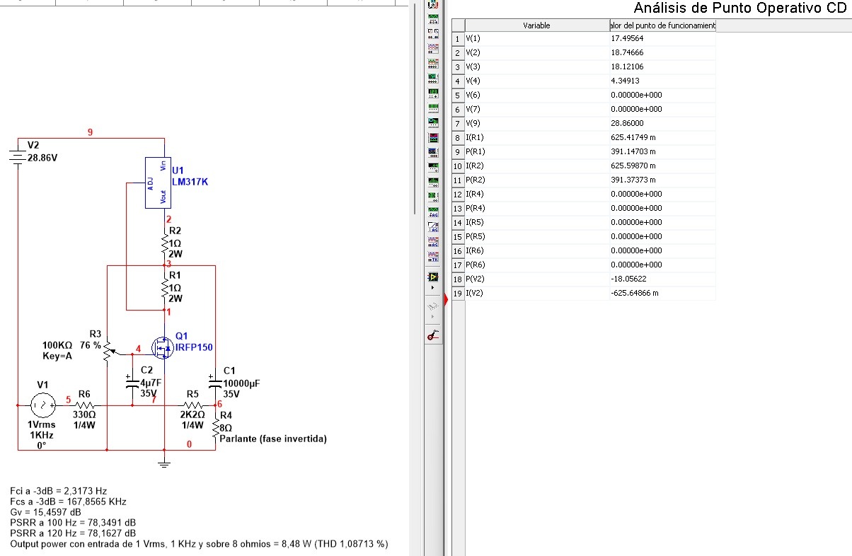
I have been working to convert the mythical Nelson Pass amplifier into a simpler one, with the addition of the well-known LM317 voltage regulator, in a curious way of operation. The result is surprisingly good.
Only 9 components, not counting those of the power supply.
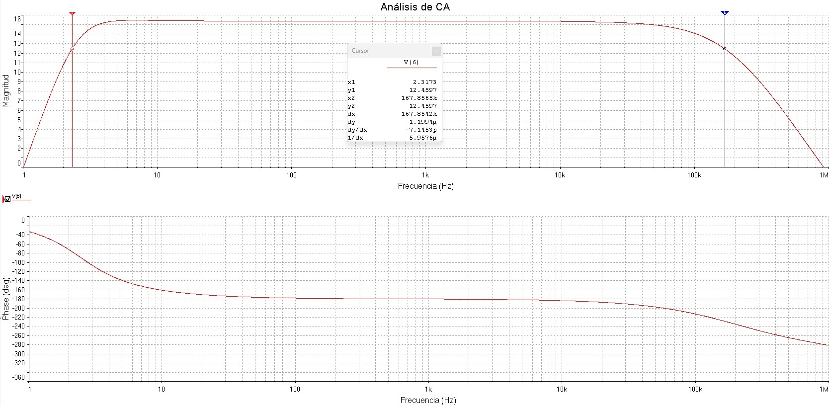
Bode:
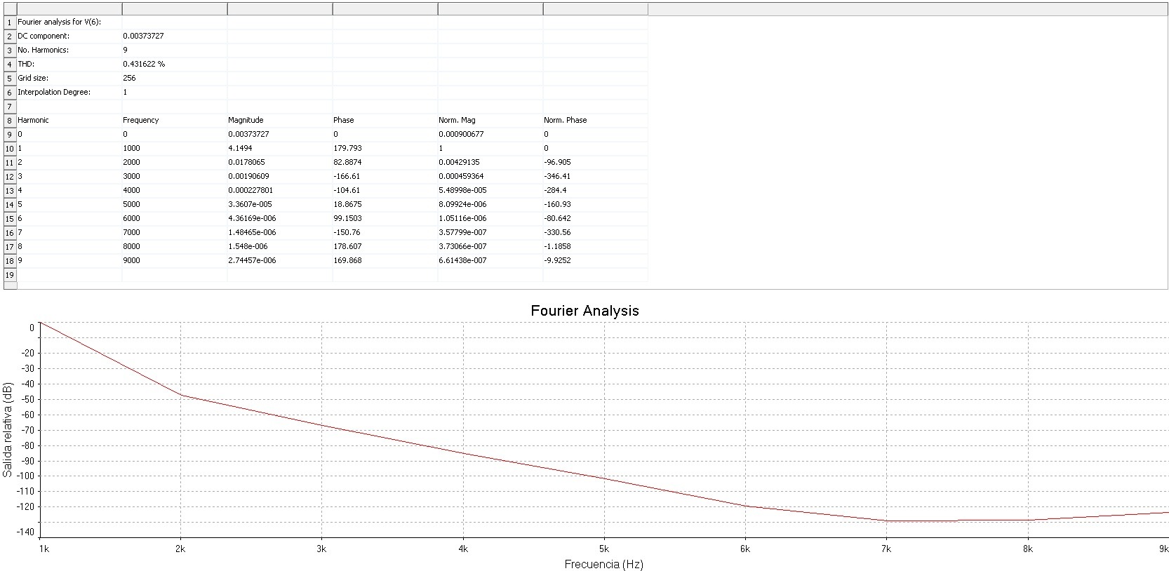
Distortion profile envelope at 1W @ 8 ohms and 1 KHz:
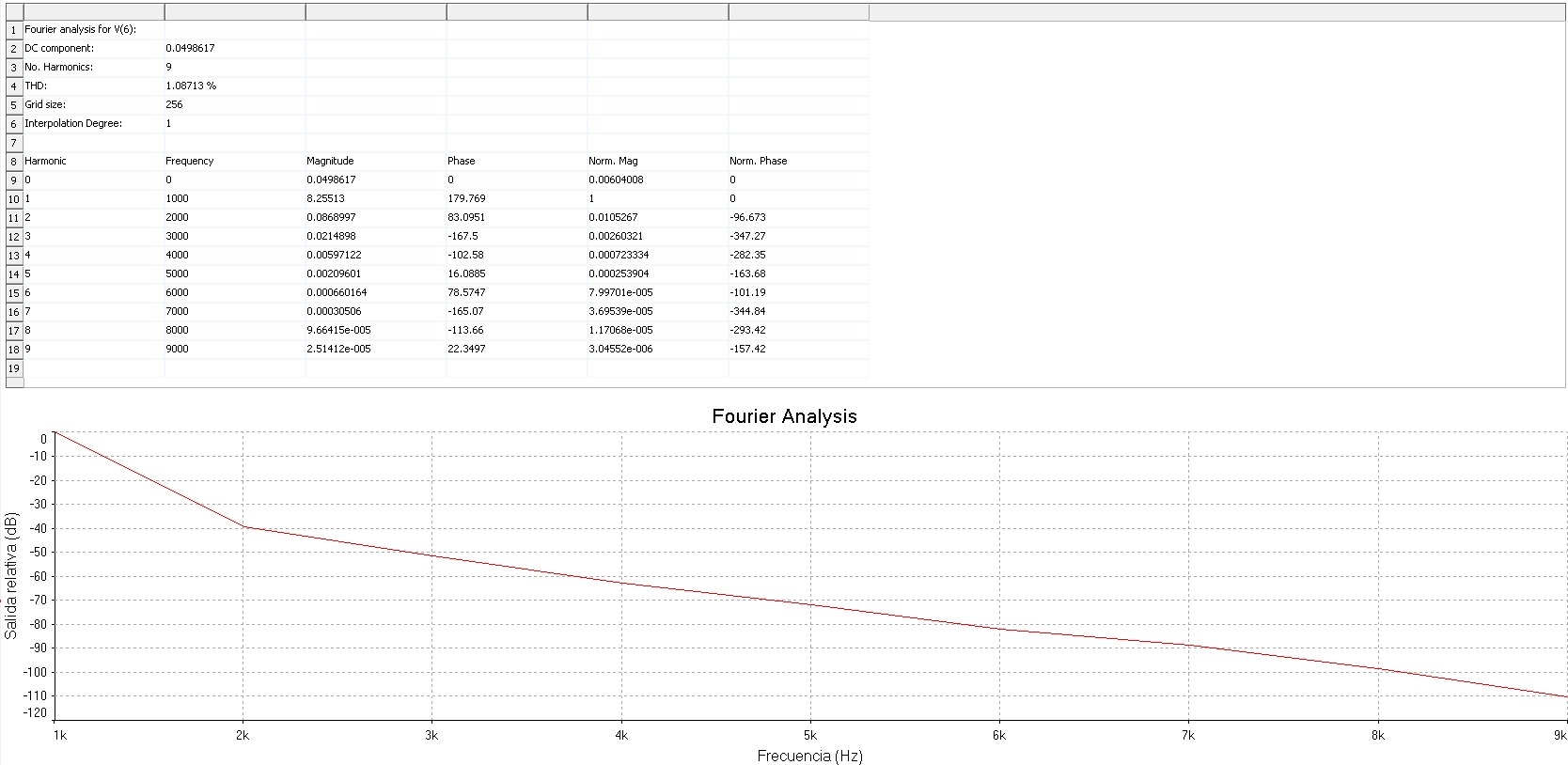
Distortion profile envelope at 8,48W @ 8 ohms and 1 KHz:
PSSR:

DC parameters:
Best regards
Only 9 components, not counting those of the power supply.
Bode:
Distortion profile envelope at 1W @ 8 ohms and 1 KHz:
Distortion profile envelope at 8,48W @ 8 ohms and 1 KHz:
PSSR:
DC parameters:
Best regards
Clever use of LM317. But why not LM1084 ?
Gives you a choice to increase bias, reduce Zout, and run closer to rail.
Patrick
Gives you a choice to increase bias, reduce Zout, and run closer to rail.
Patrick
Any option that minimizes the drop-out is welcome. Anyway, I built it with recycled elements and very easy to get.
The circuit is very versatile. Its parameters are very stable with temperature, so I suspect it would not be impossible to eliminate the output coupling capacitor using a symmetrical power supply.
It is very pleasant to listen to, due to its characteristic single ended distortion profile.
Diego
The circuit is very versatile. Its parameters are very stable with temperature, so I suspect it would not be impossible to eliminate the output coupling capacitor using a symmetrical power supply.
It is very pleasant to listen to, due to its characteristic single ended distortion profile.
Diego
LM1084 also very easy to get and not expensive.
And you can go much higher rail and bias with 3x LM317HV in parallel.
https://www.diyaudio.com/community/threads/firstwatt-j2.151909/post-7432355
Cheers,
Patrick
And you can go much higher rail and bias with 3x LM317HV in parallel.
https://www.diyaudio.com/community/threads/firstwatt-j2.151909/post-7432355
Cheers,
Patrick
Although I have not tested it on the test bench, I had already simulated using several LM317s in parallel with excellent results.
Cheers,
Diego
Cheers,
Diego
The displayed curves are the result of simulation. Although it is already tested in a very precarious way (you can see the videos), I will upload exhaustive measurements when I have more time (using applications like REW, for example).
I was able to check the stability of the current and the value of VCC/2 prior to the ELNA output capacitor.
The test was done with 2.2 ohm power resistors (that's why you see four of them to form 2 of 1.1 ohm each). Since I didn't have a 100K preset, I used a 220K one (although that change is not critical).
The real test was with 20V instead of 28 or 29V.
Last edited:
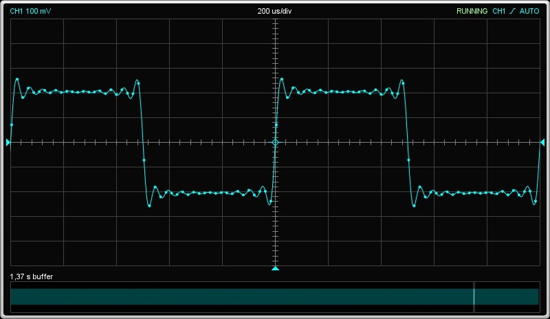
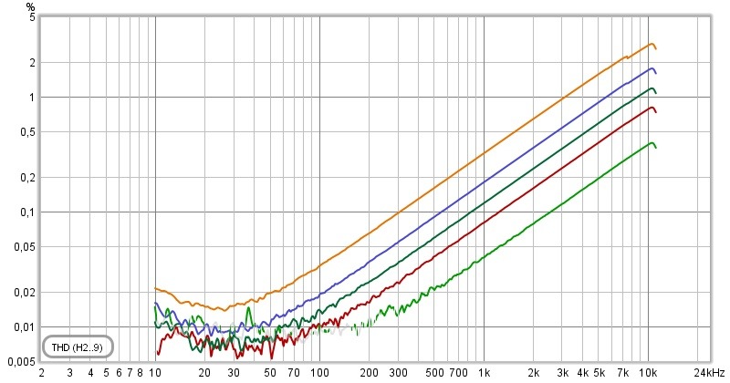
Some tests, attenuating the output at a rate of approximately 10 times, to capture with the sound card
For reference, - 12 dBFS on the input corresponds to 1.174 V RMS on the amplifier output.
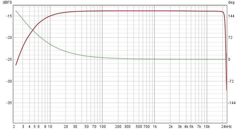
16 Hz:
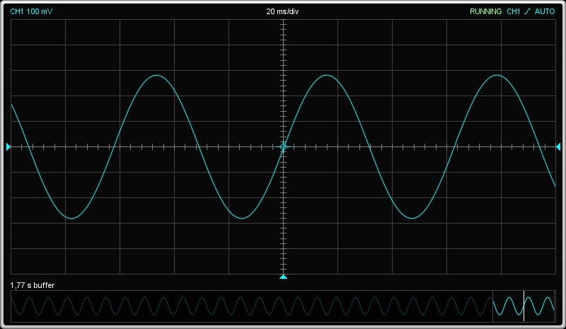
1 KHz:
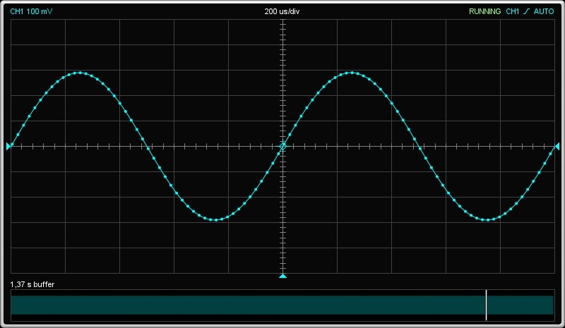
16 KHz:
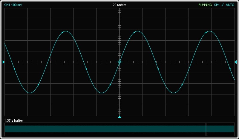
1 KHz:
Botton curve = - 15 dBFS; - 12 dBFS; - 9 dBFS; - 6 dBFS; Top curve = - 3 dBFS:

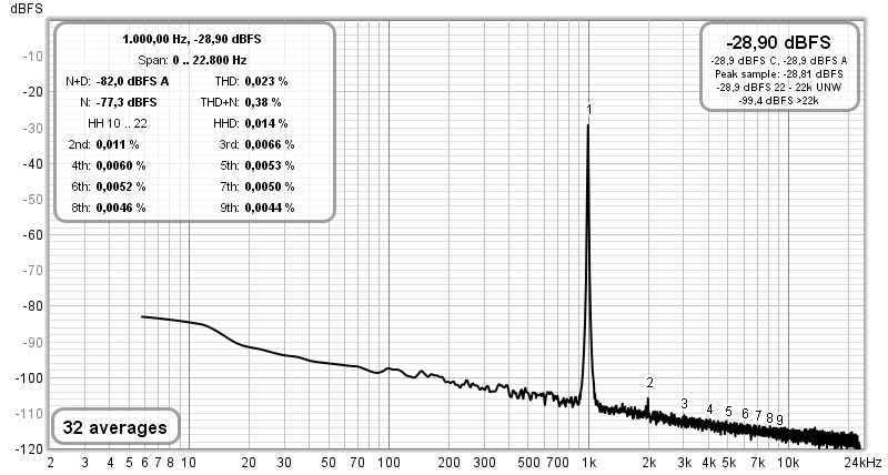
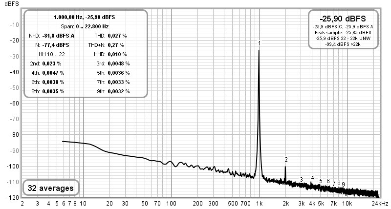
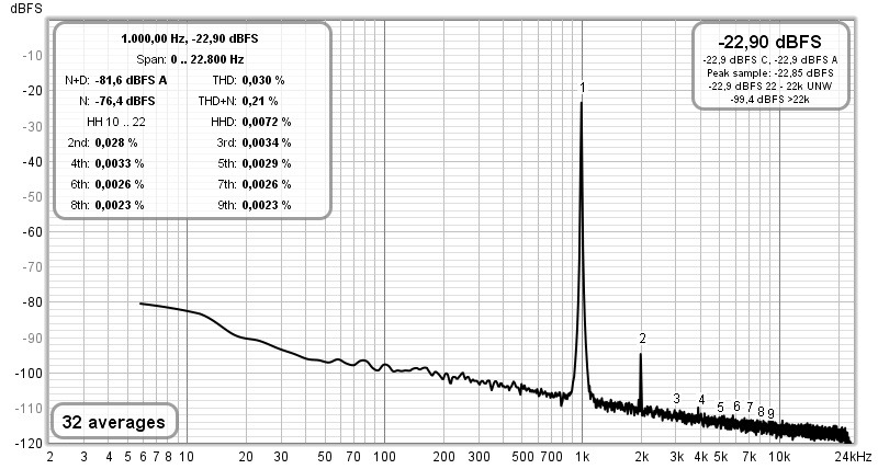
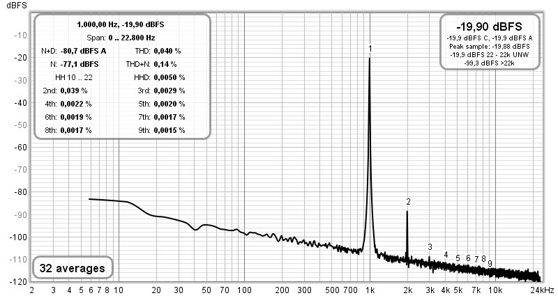
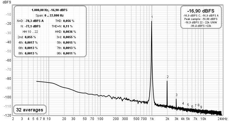
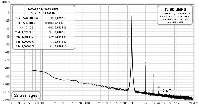
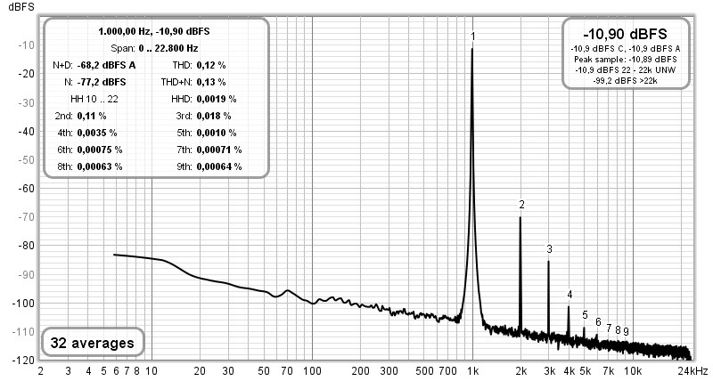
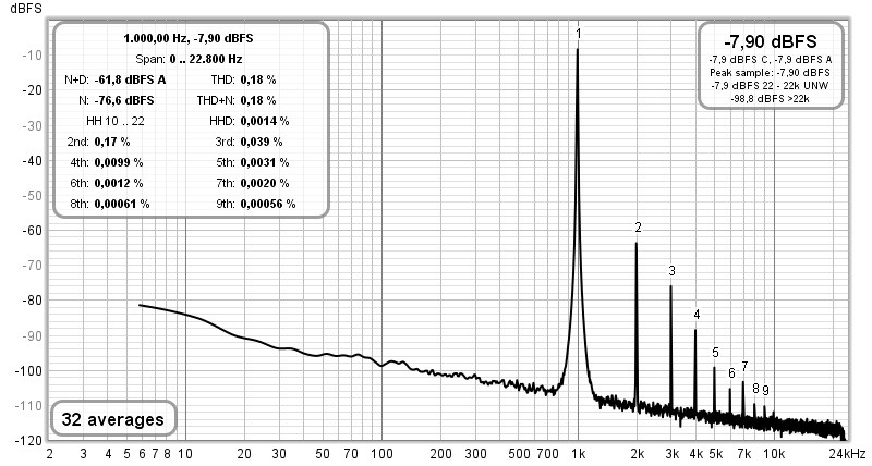
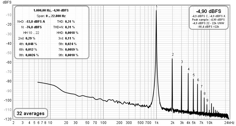
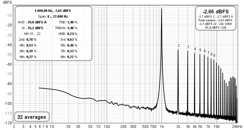
For reference, - 12 dBFS on the input corresponds to 1.174 V RMS on the amplifier output.
16 Hz:
1 KHz:
16 KHz:
1 KHz:
Botton curve = - 15 dBFS; - 12 dBFS; - 9 dBFS; - 6 dBFS; Top curve = - 3 dBFS:
Comparison test sound:
Single ended with LM317:
Comercial LG Amplifier LH-D6245A:
Single ended with LM317:
Comercial LG Amplifier LH-D6245A:
Nice work Diego
Since there are tons of 19Vdc available, would your circuit work well and be stable at 19V instead of 29V? Your harmonics profile looks great, amplifiers like yours normally sounds great and I really enjoy building them.
Even if there’s only a few components, are you aware if someone has created a PCB for it ?
Thanks
Eric
It’s a little low, was hoping for about 5W into 8 ohm. Could you please tell me if any components value would need to be changed if using a single polarity 24V supply. Also, to get such a nice harmonic profile what would be the estimated bias current. Just so I can properly size the heatsink and power supply Wattage.
Thanks
Eric
Thanks
Eric
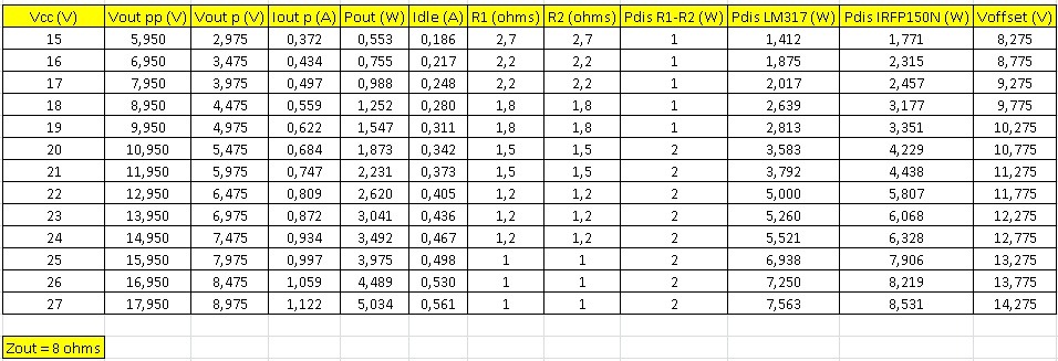
With a supply voltage of 24 Vdc, you could get around 3.5 W RMS per channel in worst conditions (much more acceptable than using 19 Vdc).
It would not be necessary to change any component, other than readjusting the voltage on the positive plate of C1, which with 24 Vdc should be around 12.77 to 12.78 V approx.
The idle dissipation of the mosfet will then be 7.6 W and that of the LM317 around 6.62 W.
Best regards
It would not be necessary to change any component, other than readjusting the voltage on the positive plate of C1, which with 24 Vdc should be around 12.77 to 12.78 V approx.
The idle dissipation of the mosfet will then be 7.6 W and that of the LM317 around 6.62 W.
Best regards
Last edited:
Only as a guide for those who wish to adapt it to their possibilities:
Best regards
Best regards
Why is your Vout pp so low, it’s about 10V below Vcc.
Could we increase the bias, seems low.
Thanks
Eric
Could we increase the bias, seems low.
Thanks
Eric
Why is your Vout pp so low, it’s about 10V below Vcc.
Could we increase the bias, seems low.
Thanks
Eric
In my bench tests, I have used around 20 Vdc for the power supply (due to the limited heatsink), so I can measure around 12 Vpp over the load without appreciable clipping. I have reached close to 16 Vpp, but with obvious cuts.
The table I uploaded includes an additional margin of safety so that the distortion profiles remain adequate for what it was designed for (single-ended character throughout its excursion, with predetermined cadence in its distortion profile and predominance of H2 over the higher ones). ). It is a more conservative table in terms of power expectations.
The voltage drop that I considered for the LM317 plus the voltage drop in one of the power resistors was 3.75 V, while for the mosfet (plus the voltage drop in one of the power resistors) was 5.3 V.
I've created a PCB with Kicad but have not used it yet and won't get around to it until November. Gerbers attached. Let me know if you find mistakes.
View attachment 1219170
View attachment 1219172
In the schematic that you have kindly uploaded, I can see that the source terminal of the mosfet is not connected to 0V as it should. I have not been able to check if that is correct on the PCB that you kindly designed.
Thank you for your job!!!.
Best regards
- Home
- Amplifiers
- Pass Labs
- Hybrid ZEN Amplifier + LM317 = Efficient and simple