Sorry, but - no. As I get it, I dare to say: A current source as the plate load forces the triode to operate with (almost) constant plate current, hence with a voltage gain next to it's µ - which basically is very good, but in turn leads to a rather high Miller capacitance in parallel with the cartridge. Due to it's very high input impedance, there's no signal current leaking into the 2nd FET. It's driven by the signal voltage that appears at the plate, amplifying it additionally. Yes, the NFB to the cathode results in a rather low output impedance, which again is very good.
If you'd want almost no AC voltage at the input triode plate, you'd need a Cascode, either with a 2nd triode or a SS device. Nothing against loading that Cascode with a CCS as a 3rd device, it will result in a pentode-like voltage gain, if needed.
Best regards!
If you'd want almost no AC voltage at the input triode plate, you'd need a Cascode, either with a 2nd triode or a SS device. Nothing against loading that Cascode with a CCS as a 3rd device, it will result in a pentode-like voltage gain, if needed.
Best regards!
That's not how it works at all - remember the feedback.
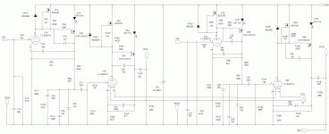
I use this gain cell all over the place with various permutations and combinations of tubes and semis. I used to include a cascode between the plate/drain and the current source for RIAA input duty because of fears of multiplication of Miller capacitance. I then bothered to monitor the voltage between plate/drain and the current source in simulation. I found that the first stage voltage gain was about 0.3 - most of the amplification is taking place in the output p-channel.
If I remember, I'll include a simulation showing that. Perforce it will be a semiconductor-based gain cell, but it will show the basic principle of operation.
 !
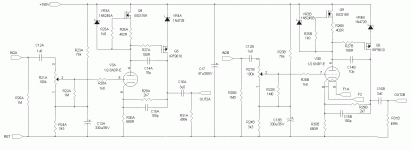
!Here's a gain cell using a jfet and a couple of mosfets as an example - I have set a probe in place at the jfet drain using a 1uF cap and 1M (1000k - Orcad PSpice doesn't like "m"). Input excitation level is 0.1V. As seen in the simulation results, signal at the jfet drain is a mere 40mV , for a first stage gain of 0.4 - feedback in action.
BTW - I re-ran the sim with a probe impedance of 20M just to rule out any obscure loading effect, and the result is the same...
BTW - I re-ran the sim with a probe impedance of 20M just to rule out any obscure loading effect, and the result is the same...
Attachments

Last edited:
I am not sure that the current source load is actually required -
if you are at it you may want to simulate with a resistor instead
and leave away D1. Most of the time a scheme like this is used
with a pnp as second stage and so it is obvious that plate voltage
is held "constant".
if you are at it you may want to simulate with a resistor instead
and leave away D1. Most of the time a scheme like this is used
with a pnp as second stage and so it is obvious that plate voltage
is held "constant".
The current source has beneficial results for THD over a resistive load, as its impedance is much higher. I started out in circuits of this type using a resistive load, but switched to the current source due to the benefits. The BSS159 is especially nice in this regard as it has relatively low capacitance. D1 is also a "component with benefits", as you get the voltage drop without a lot of associated impedances. Both tricks increase the open loop gain and lower distortion as a consequence.
Check out this thread, and you can see the benefits of all the tricks used together...
BSS159 Line Amp
Check out this thread, and you can see the benefits of all the tricks used together...
BSS159 Line Amp
Last edited:
I am not sure that the current source load is actually required -
if you are at it you may want to simulate with a resistor instead
and leave away D1. Most of the time a scheme like this is used
with a pnp as second stage and so it is obvious that plate voltage
is held "constant".
Yes, with the low input impedance of a PNP, maybe even without an emitter resistor, it is really obvious.
German TT manufacturer did something like this, but with swapped sexes, in their TVV 47 four-transistor design.
Best regards!
You can take out the current souce and led/zener, and end up with a design that I abandoned 5 years ago, with lower open loop gain and higher distortion.
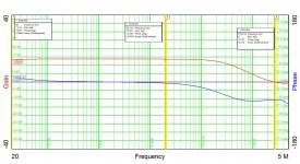
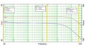
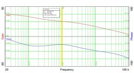
Here's the result of the lastest encounter of the line stage with the gain-phase analyzer at work. The extra compensation capacitor does its job and forces the gain below 0dB.
I'll post final schematics when I get the reference designators for the extra compensation caps sorted out.I decoded to treat all the stages of this preamp with the same compensation scheme as the line stage. As can be seen from the scans, gain for the line stage is very stable and repeatable.
I'll post final schematics when I get the reference designators for the extra compensation caps sorted out.I decoded to treat all the stages of this preamp with the same compensation scheme as the line stage. As can be seen from the scans, gain for the line stage is very stable and repeatable.
Attachments
I plan to try one more compensation option that may allow use of one compensation capacitor. Hopefully this option will allow the gain to cross through 0 dB with adequate phase and gain margin.
More later....
More later....
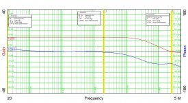
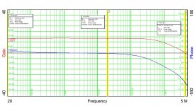
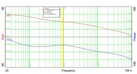
OK, I ran the line amp gain-phase scan this afternoon with a single 47pF compensation cap strategically placed, and came up with this result.
0 dB crossover is at a respectable frequency, and there's enough phase margin for stable operation, though with not quite as much margin as I'd like. I think the way forward would be to ad a series resistor to the compensation cap to break the pole somewhat From my calculations and the data shown here, I would try somewhere between 1-1.5k. I'll try it next week when I have a little more time to play with the gain-phase analyzer.
0 dB crossover is at a respectable frequency, and there's enough phase margin for stable operation, though with not quite as much margin as I'd like. I think the way forward would be to ad a series resistor to the compensation cap to break the pole somewhat From my calculations and the data shown here, I would try somewhere between 1-1.5k. I'll try it next week when I have a little more time to play with the gain-phase analyzer.
Attachments
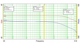
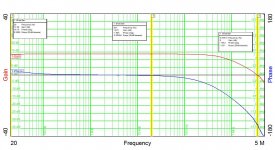
This weekend, I investigated the effects of a 1k resistor place in series with a single strategically placed 47pF compensation capacitor on the line amp section of the preamp. Attached are gain-phase plots of the left and right channels.
Both channels show better phase margin with a 47p + 1k series network over a 47pF cap by itself. Strange to relate, the phase margin on CH1 is less for that of CH2. This might possibly be due to a differnece in gate capacitance between the two output p-channel mosfets. I might look at using the same p-channel output device I'm using on the RIAA gain blocks for the line amp, if I can manage the power dissipation. The SMD device I'm using in the RIAA gain blocks has substantially less gate capacitance than the IRF9610 fets I'm using for the line stage. More on that late, after I dig in and analyze the power dissipation of the line stage. As an unexpected bonus, I may be able to reduce the overall power consumption of the preamp, which draws ~12W of power for all stages off the +150V supply.
Both channels show better phase margin with a 47p + 1k series network over a 47pF cap by itself. Strange to relate, the phase margin on CH1 is less for that of CH2. This might possibly be due to a differnece in gate capacitance between the two output p-channel mosfets. I might look at using the same p-channel output device I'm using on the RIAA gain blocks for the line amp, if I can manage the power dissipation. The SMD device I'm using in the RIAA gain blocks has substantially less gate capacitance than the IRF9610 fets I'm using for the line stage. More on that late, after I dig in and analyze the power dissipation of the line stage. As an unexpected bonus, I may be able to reduce the overall power consumption of the preamp, which draws ~12W of power for all stages off the +150V supply.
Attachments
Last edited:
I've done a new layout with the new compensation scheme and using the SMD p-channel FET on all channels. Any results I present form henceforth will use the new configuration and layout.
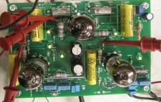
New boards are in, and I'm busy populating them. More results when I finish stuffing the boards and powering them up...
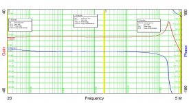
Yesterday I got a reminder not to count my chickens before they hatch... I was running gain-phase scans on both the RIAA and line sections of the preamp using the latest layout. The RIAA sections match to within 0.1 dB. The line sections looked radically different regarding gain-phase near crossover, with one channel showing a weird peaked response with rapidly crashing phase at a few MHz. This looks to be the consequence of using surface mount instead of TO-220 p-mosfets for the line amp output stage. The heat sinking land for one side of the line stage extended under the input coupling capacitor, causing positive feedback and a peaked response at high frequency. Also, I did some viewing with a thermal camera, and the output mosfets on some of the RIAA gain blocks are a bit too hot for my taste.
To fix this, I am going to take all the output p-channel output fets for the gain blocks off the main board and move them to identical small daughter cards with adequate PC land heat sinking. These will be located so that they can't cause any feedback problems. I'll be using 3-pin right angle headers to connect the daughter cards to the main board with adequate support. I may also go back to my original compensation scheme. It was a bit more complex, but gave me excellent and controllable phase margin.
To fix this, I am going to take all the output p-channel output fets for the gain blocks off the main board and move them to identical small daughter cards with adequate PC land heat sinking. These will be located so that they can't cause any feedback problems. I'll be using 3-pin right angle headers to connect the daughter cards to the main board with adequate support. I may also go back to my original compensation scheme. It was a bit more complex, but gave me excellent and controllable phase margin.
Attachments
Last edited:
Layout is proceeding for the new board version with daughter cards for the output mosfets. Once I sort out the reference designators on the new mother board, I can design the daughter cards. I'll be including the gate stopper resistors on the daughter card along with the mosfet.
- Home
- Source & Line
- Analogue Source
- Hybrid RIAA/Line Amp