
Fixes a couple of idiot stuffing errors yesterday. Will try biasing up the amp again this coming week.
The RIAA part of the preamp is biasing up nicely, but one channel of the line amp is being stubborn. More later as I diagnose and fix the problem.
I just found the layout stupidities that kept one side of my line amp from biasing up properly. Deft work with a Dremel is indicated.
Dremel work is done, and I replaced al the semiconductors on that side of the line amp (they probably had a vey bad time of it). I'll try to cautiously bias up the preamp again later today.
Dremel work is done, and I replaced al the semiconductors on that side of the line amp (they probably had a vey bad time of it). I'll try to cautiously bias up the preamp again later today.
Dumb-a** mistakes corrected, line amp now biases up correctly. I'm changing a couple of values on the RIAA 40X stage to bring down the temperature of the p-channel mosfets there. After that, it's time to measure...
It's About Time..
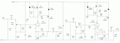
I finally got the dumb mistakes fixed on my board, so it was measurement time this afternoon. Attached are gain-phase scans of the RIAA and line amp sections.
Response curves for the RIAA preamps are very well-matched as a consequence of programming in excess gain for each section and using feedback.
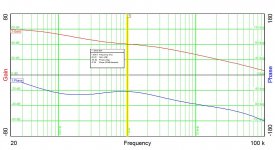
The line amps are also well-matched, but rolled off a little bit earlier than I expected, likely due to using a 1k instead of 100 ohm gate stopper for the IRF9610 p-channel fets. THe gain does not pass through zero for the line amps as well, so a second compensation cap is indicated. The time domain response of the line amps will likely look just fine, but I expect the gain to roll down through 0dB at crossover and stay below 0dB. Otherwise, the amps might be only conditionally stable.
I finally got the dumb mistakes fixed on my board, so it was measurement time this afternoon. Attached are gain-phase scans of the RIAA and line amp sections.
Response curves for the RIAA preamps are very well-matched as a consequence of programming in excess gain for each section and using feedback.
The line amps are also well-matched, but rolled off a little bit earlier than I expected, likely due to using a 1k instead of 100 ohm gate stopper for the IRF9610 p-channel fets. THe gain does not pass through zero for the line amps as well, so a second compensation cap is indicated. The time domain response of the line amps will likely look just fine, but I expect the gain to roll down through 0dB at crossover and stay below 0dB. Otherwise, the amps might be only conditionally stable.
Attachments

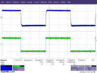
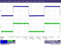
Before I mess with the compensation values on the line stage, I'll run a time domain response (probably tomorrow) to see how it looks. I'm expecting the response to be a bit on the slow side.
I expect things will perk up considerably when I replace the stoppers on the IRF9610s with 100R from the current value of 1k. I'm also considering backing off the compensation caps, changing the current value of 220p to 100p. This will likely push the zero crossing frequency past the 5MHz capability of the Venable gain-phase analyzer available at work.
I expect things will perk up considerably when I replace the stoppers on the IRF9610s with 100R from the current value of 1k. I'm also considering backing off the compensation caps, changing the current value of 220p to 100p. This will likely push the zero crossing frequency past the 5MHz capability of the Venable gain-phase analyzer available at work.
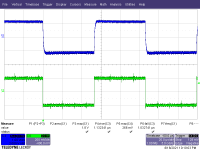

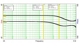
From the look of the time domain response in post #28, one might assume that everything is hunky-dory and stable with the line amp. However, the gain-phase plot shows differently, with the response never going below 0dB and even starting to turn up. Conditional stability...
Lesson learned from this - a clean time domain response is a necessary condition for stability, but it doesn't guarantee stability on its own.
Lesson learned from this - a clean time domain response is a necessary condition for stability, but it doesn't guarantee stability on its own.
I'll be adding a couple of 10pF capacitors to the line stage compensation, and will be running gain-phase plots this weekend. When the dust settles, I'll be posting appropriately modified schematics. I may add the extra compensation to the RIAA gain blocks as well.
Through the course of this thread, people have been asking for schematics - schematics have been offered, with zero commentary. Was this not what you expected to see? What is going on...
Feel free to comment, though you may not necessarily get the answer that you like. I follow my own muse in design, and what I post here is a courtesy for folks who might like to follow along with what I'm doing.
Feel free to comment, though you may not necessarily get the answer that you like. I follow my own muse in design, and what I post here is a courtesy for folks who might like to follow along with what I'm doing.
...people have been asking for schematics - schematics have been offered, with zero commentary.....
Wasn't it just Kay?
Follow your own muse. You seem to be doing good.
Somebody else also piled on early in the game.
If I like the gain-phase plots this weekend, this board is getting a case and some knobs. Next up will be designing the DC-DC to power it. I have the choice of using a Baxendall converter with a buck front end to power this, or using a modulated current source instead of a buck inductor - perhaps quieter, but loads less efficient. I tried the current source-driven Baxundall oscillator back in 1981 or so when designing a 1500V oscilloscope power supply. It worked OK, but one thing I didn't realize back then was that the Baxendall converter needs a high-leakage transformer to function properly. I opted back then for a choke input filter, which also isolated the primary tuned circuit sufficiently to allow proper operation. I also know a lot more about switching power supply control loops, so that would be a help here as well.
If I like the gain-phase plots this weekend, this board is getting a case and some knobs. Next up will be designing the DC-DC to power it. I have the choice of using a Baxendall converter with a buck front end to power this, or using a modulated current source instead of a buck inductor - perhaps quieter, but loads less efficient. I tried the current source-driven Baxundall oscillator back in 1981 or so when designing a 1500V oscilloscope power supply. It worked OK, but one thing I didn't realize back then was that the Baxendall converter needs a high-leakage transformer to function properly. I opted back then for a choke input filter, which also isolated the primary tuned circuit sufficiently to allow proper operation. I also know a lot more about switching power supply control loops, so that would be a help here as well.
Yes, the last one was me. But admittedly I just don't get what these semiconductors, especialy the LED's, at the plates do. And I'm rather keen on feedback designs to have the impact of tube tolerances and ageing decreased.
But who am I to say do this instead of that and so on?
Best regards!
But who am I to say do this instead of that and so on?
Best regards!
Last edited:
Slowly, but steadily I'm getting it. Initially I had overlooked that the FETs are of different sexes and asumed the last ones are source followers, which they aren't. So it is clear to me now why this is a NFB design  .
.
Best regards!
.Best regards!
In the schematics, the topside BSS159 is a depletion mode fet used as a current source to set up the bias for the 6N3P-E triode. The current source is clamped by a zener to prevent an overdriven triode from popping the gate of the p-channel fet in the 2nd stage.
The led (or zener) in the source of the p-channel device acts as additional low-impedance voltage drop so that the depletion mode current source has enough voltage across it for proper operation. Use of an LED or zener provides the voltage drop with relatively low incremental impedance, so there is not much degeneration applied to the source of the p-channel fet, maximizing open-loop gain.
Use of a current source load on the triode forces it to operate at almost constant voltage, as any attempted change in triode operating current gets passed right to the p-channel output device and applied as negative feedback to the cathode of the triode. The actual gain of the triode in the circuit is less than one, so a cascode won't be needed to reduce the triode Miller capacitance, even for the RIAA preamp input.
The high degree of negative feedback results in low output impedance.
Use of feedback results in more consistent operation - this is shown on the gain-phase plots of the RIAA preamps. The 1kHz gain of each channel is pretty much perfectly matched.
Last edited:
- Home
- Source & Line
- Analogue Source
- Hybrid RIAA/Line Amp