Measure cold at 130mV and warm at 200mV, would it reach 50C when in use I'd put it on the low table where I lay my feet and use it as a warm up device with this damn cold weather...
I think you'll find that the F4 is a very fine amp once you get the output stage biased properly, and can feed the input with enough voltage swing / gain. You can go as high as... maybe 300mV across the source resistor. BUT, this depends on the thermal performance of your heatsinks and proper ventilation. 50C is OK, don't go any higher than 55C. You should be able to keep your hand on the heatsink indefinitely at thermal equilibrium. Performance of the amp gets better as you increase the bias current through the power MOSFETs. When you are setting up one of these Class A amplifiers, be very patient and take your time with it. Walk the bias and DC offset pots slowly, back and forth. Allow some time between the adjustments. Run 2 multimeters at the same time, so you can keep track of what's going on.
I so much wanted to check the bias this morning, took the amp cover off and worked my best to find the above mentioned resistors to measure but to my luck the probes of my DMM won't fit 🙁 do you have some suggestions to work it out?
What else could I measure to check it being properly biased?

What else could I measure to check it being properly biased?

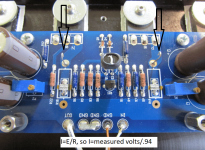
Here's how I personally did it (see attached pictures). I soldered some test points to the board and measured across two of the series resistors. We live and breathe ohm's law around here so you know it's I=E/R. We find the current through something by measuring the voltage across it, and we already know that we have .47 ohm resistors. So, you take the reading, and do the math. So, I clipped the voltmeter to the test points on my pcb, took note of the voltage reading, then did the math to find the current through that leg of the output stage. The F4 has three legs, or what we refer to as being a "3 deep" output stage. My math was... current=.55 volts divided by .94 ohms. My own personal F4 had a total of 1.75 amps of bias current (.58A per leg).
Attachments

Last edited:
Source pins of mosfets are exposed enough (pin, most right one, when mos is looking with numbers at you, pins down)
so, connecting one probe to 240 Source pin and second probe to 9240 Source pin will give voltage sag across two source resistors
so, if target figure is 280mV across one source resistor, this way readout needs to be twice that : 560mV
numbers just from top of my head , applicable for 600mA per mosfet string, resulting in sum Iq of 1A8
if desired figure is smaller, calculus is simple and most likely already mentioned elsewhere
reminder - final settings in temperature equilibrium
whatever room temperature is, means when amp is hottest ....
edit: if that is confusing, another and maybe easier way is - one probe to Source pin of mosfet, other probe to speaker output (wherever is convenient to clip probe); that's showing voltage sag across one 0R47
Last edited:
Ciao @william2001 this community never quits surprising me with both knowledge and kindness nonetheless I am a total nerd all of you been very kind with suggestions.
So, if I get it right, I can use the probes like in the attached pic and then make the maths and/or report the readings here as suggested by @cubicincher.
No matter the order, I can start from back to front, correct?

So, if I get it right, I can use the probes like in the attached pic and then make the maths and/or report the readings here as suggested by @cubicincher.
No matter the order, I can start from back to front, correct?
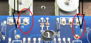
ZM is right, measurement has to be from the N channel to the P channel, the Source pins. Not like your picture.
Attachments
Last edited:
Ok, with the mosfet facing me (the right one in the pic) I take measure from source and speaker output on the same bank, repeat procedure for each and every source pin (which is the opposite on the other side of the board, left in the picture)?Source pins of mosfets are exposed enough (pin, most right one, when mos is looking with numbers at you, pins down)
so, connecting one probe to 240 Source pin and second probe to 9240 Source pin will give voltage sag across two source resistors
so, if target figure is 280mV across one source resistor, this way readout needs to be twice that : 560mV
numbers just from top of my head , applicable for 600mA per mosfet string, resulting in sum Iq of 1A8
if desired figure is smaller, calculus is simple and most likely already mentioned elsewhere
edit: if that is confusing, another and maybe easier way is - one probe to Source pin of mosfet, other probe to speaker output (wherever is convenient to clip probe); that's showing voltage sag across one 0R47

Last edited:
Giovanni,
I'm very happy you are taking the plunge and doing some measurements.
The red circled pins in post #29 from William are the 'Source' pins. ( FYI, I've attached the pinouts of the IRFP240; IRFP9240 has the same pinout as well. )
So keep one meter probe on a channel's positive output (doesn't really matter which probe; you can just screw it in the binding post). Use the other proble and measure the voltage at the Source pins of every IRFP240/IRFP9240 for that channel, and write them down. You will see some as positive and some negative. Don't worry about it. When you have done so, please report back.
Cheers,
Dennis
Attachments

Ok, with the mosfet facing me (the right one in the pic) I take measure from source and speaker output on the same bank, repeat procedure for each and every source pin (which is the opposite on the other side of the board, left in the picture)?
View attachment 1144617
you need to make amp Iq setting observing just one ( any of 6) source resistors
also, do not forget observing and setting output DC Offset (Vdc meter across speaker outputs)
when done, you can check voltages across all 6 source resistors (moving just red probe to each of 6 source pins, black probe staying at speaker output), to check how well mosfets are matched
Right channel bank:
left to right probe on the left leg of the mosfet I read 4.5 - 4.5 - 4.5 (dropping below 4.4 after a few minutes) on the following three I inverted the probes to keep the reading positive and have 1.10 - 1.06 - 0.92
Left channel bank:
here I have 0.71 - 0.75 - 0.76 and 4.4 and dropping on the other three
What am I doing wrong?
edit: putting probe on the right leg of all of the mosfets on the right channel bank I get very similar readings and all of them slowly dropping since I switched it on
With probes on the speakers output and meter on 2v range I measure 0.13v
Last edited:
measuring Iq:
also, you need to re-set output DC offset, when amp is hot; 130mV is too much, try to set it closest to 0mV you can
one probe to Source pin of mosfet, other probe to speaker output (wherever is convenient to clip probe); that's showing voltage sag across one 0R47
also, you need to re-set output DC offset, when amp is hot; 130mV is too much, try to set it closest to 0mV you can
Good thing ZM remembered to ask about the DC offset. 0.13V is indeed too high and certainly makes me wonder how well the amp was adjusted during its original construction. 🙁
Something must be wrong with the DC offset, right channel being 8.5mV and left being 31.5mV 🙄
I should act on P2 to adjust the offset, is that correct? How do I do, clip the probes on the speakers output of each channel and turn unti, on the 200mV scale, I get down to where, the closest to 0mV as per above ZenMod suggestion?
I checked one bank of the amp, transistor source leg to speaker output and I get a range from 100mV to 124mV, DC offset being 7.6mV
I am following yours all instructions as well as on the first page of the building guide, sorry but I am no tech at all, I am just taking readings and going through trial and error not to say that English isn't really my mother tongue
Last edited:
please re-read how to measure and what to measure
according to figures you gave us in last few posts, I'm sure that you still don't know what you're doing .....
everything is clearly written
according to figures you gave us in last few posts, I'm sure that you still don't know what you're doing .....
everything is clearly written
Left to right readings on the right leg of the transistor after I'd say an hour or more, case is cold:
108 - 102 - 120 - 124 - 113 - 99 mV
OK, now we're getting somewhere. This amp is not biased properly. No wonder it doesn't sound great. As I mentioned before, use two voltmeters at the same time. Keep one on the speaker outputs to watch DC offset, adjust DC offset pot to get 0.0mV at the speaker terminals (some wiggle is OK) as needed while messing with the bias pot. Put the other voltmeter exactly as you did in post #38. Adjust bias pot to get ~200mV across one of those resistors, any one, it doesn't matter which. Now let it cook and watch the heatsink temperature. Be patient with it, this is a slow process.
Last edited:
now, look and read here : https://www.diyaudio.com/community/threads/f-4-boards.214003/
clip red probe to (any) source pin, black probe to speaker positive output
in small steps, rotate P1 and set to reding of 200mV on your DVM, when amp is hottest
do the same for other channell
then - with DVM across speaker terminals, small steps on P2, set output DC offset as close to 0mV you can
inputs shorted, no load on output
- Home
- Amplifiers
- Pass Labs
- How to turn a dual mono F4 into a mono block?