I wonder why the original manufacturer did not simplify that way in the first place, there must be a reason why they have preferred individual components.
It has been known for loudspeaker manufacturers to make bulk purchases of components which are available at a good price. Perhaps they had a large stock of 4.7 ohm resistors and 100 uF capacitors to use up! 😉
P.S. An LCR meter (as attached) is a useful tool for crossover constructors.
Attachments

I see that Intertechnik (from where your 5.6 mH inductor originated) also does crossover development boards under the name of BlockBoard.
They have a selection of sizes, e.g., https://www.intertechnik.com/shop/circuit-boards/ite-blockboard-lp05,583193,en,8067,1159099
They have a selection of sizes, e.g., https://www.intertechnik.com/shop/circuit-boards/ite-blockboard-lp05,583193,en,8067,1159099
Hi Folks,
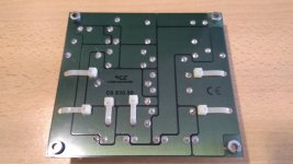
Eventually, I found some time to draw the PCB for the parallel notch filter I attached in post #67.
Here some images to give you an idea:


I have a few questions:
Alex
Eventually, I found some time to draw the PCB for the parallel notch filter I attached in post #67.
Here some images to give you an idea:
I have a few questions:
- Just to be sure: If you look the schematic in post #67, am I correct to think that once the filter is ready, the terminal J1 W (left on the PCB image above) will need to be wired to the terminal W on the crossover, while the terminals I marked as J2 and J3 respectively to the Top and Bottom Woofers?
- The crossover terminal market IN in post #67 will be wired to the banana plugs of the speakers.
- Why the filter polarities in the schematic in post #67 are inverted vs the rest of the W circuit? Essentially, the - will end in a + in the crossover and vice-versa.
Alex
The woofers are wired in reverse electrical phase to ensure they will be acoustically in phase with the mid and tweeter. This is necessary because of phase changes introduced by the crossover components.
EDIT: I'm copying the schematic from post #67 here for comparison in the hope that someone else can comment on your two other statements!

EDIT: I'm copying the schematic from post #67 here for comparison in the hope that someone else can comment on your two other statements!
Last edited:
This may help, but in principle the schematic should be good, I just need to be sure on the wiring once I have finalized the PCB.

I have used filled areas for consistency with the original crossover from the manufacturer.
I have used filled areas for consistency with the original crossover from the manufacturer.
Attachments
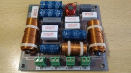
Right, I've re-read your questions and see that I also need to look at the physical layout of the whole crossover board in the photograph.

The terminal marked IN goes to the banana sockets on the back of the enclosure (the input from the amplifier).
J1W on your auxiliary board should be wired to the terminal W on the crossover board.
J2 and J3 should respectively be wired to the top and bottom woofers.
However, if you are asking me to verify that your PCB layout is correct, I'm afraid that I would find that a challenge without the board in my hands!
So essentially my initial thoughts are correct, the only open question is whether the schematic on the auxiliary board if good ot not.
I get zero errors from the electrical rule check in the schematic I designed, so I guess I should be fine.
I get zero errors from the electrical rule check in the schematic I designed, so I guess I should be fine.
Whether the physical layout of your auxilliary PCB is correct is the question.
However, I am sure that with sufficient double checking you can verify that it is.
I get dizzy trying to trace the copper traces!
However, I am sure that with sufficient double checking you can verify that it is.
I get dizzy trying to trace the copper traces!
Have you simulated this new crossover? It appears the last capacitor across the lower bass driver may tend to increase the higher frequencies to the upper woofer.
Hi,
I have not. I wouldn't know how to do it either.
Why do you think that capacitor might increase the higher frequencies to the upper woofer? The position I placed it in the PCB?
I have not. I wouldn't know how to do it either.
Why do you think that capacitor might increase the higher frequencies to the upper woofer? The position I placed it in the PCB?
As the frequency rises and reactance of the capacitor falls, the Voltage across the other woofer increases.
In other words the total drive which was split between both woofers is now going to just one of them, representing a default 6dB increase.
In other words the total drive which was split between both woofers is now going to just one of them, representing a default 6dB increase.
I decided to run a sim comparing this to the original crossover. It's not accurate as it uses blank driver files, and the large high pass capacitor interaction with the peaks isn't shown.
However it does indicate a rise at the top of the passband.


However it does indicate a rise at the top of the passband.
Now, maybe this is needed to go with the responses, I'm not clear on that. However this happens to be something I see a lot of when people are trying to do baffle step compensation on their two series woofers. They cut one but don't expect it will bring up the other, which defeats the baffle compensation.
@Kwajongen
I have never been worried about that 100 uF capacitor!
In simple terms, the capacitor will shunt the higher bass frequencies around the lower woofer meaning that only the lower bass frequencies will pass through, and will be reproduced by, the lower woofer - hence its designation 'basso'.
There may be more to it all, as AllenB is exploring, but the crossover designers clearly knew what they wanted to achieve and how to achieve it.
You may carry on with your auxilliary PCB in its current form.
Last edited:

Thank you all.
Yes, the schematic in post # 84 is the original from the project manufacturer, Coral/Peerless. I have no doubt it is done to work properly.
The schematic in post #1 is the one of the company who supplied me with all the components, not sure how they did it at the time, but they were a well known company, so I guess they knew what they were doing too.
Even if you a figured it out, just to dispel any doubts, in this context, Alto=Top Woofer and Basso=Bottom Woofer.
I will keep going and come back with the results.
Tank you all!
Alex
- Home
- Loudspeakers
- Multi-Way
- How to further cut the high frequencies of my speakers?