Check Q9. Its saturated, Vce is almost zero. While Q8 is not. The voltages from these bases to the rails should be almost the same. Just noticed the rails are only at 3 volts, the above may not aply till higher rail voltages.
I think the voltages are measured from different reference points.
I believe Q7 is a DN2530, which is a depletion mode mosfet and so it is normally on. I tried reducing the value of R35, but long before the amplifier is fully powered up the power rating of R33 and R34 is exceeded. So I concluded the resistor values around Q7 are at least adequate for now.
This does leave the question of the -1.93V on the base of Q8 and the 1.30V on the base of Q9. I would expect them to be the same with opposite signs. Why are they so different?
This does leave the question of the -1.93V on the base of Q8 and the 1.30V on the base of Q9. I would expect them to be the same with opposite signs. Why are they so different?
I powered the amp on again and measured voltages again. Some voltages around Q5-Q13 are now very different from when I measured them last night. The amp was on longer last night so there could some change due to temperature, though I checked at the start of my measurement and after and changes were extremely small. I'll do some more measurements today and update the thread then.
Last edited:
Are the red measured values of Q8 (2SC4793) as shown or exchanged accidentally? They are comparable with the values at Q9 (2SA1837), but just swapped! In the given result, fet-current through R31 is 1.25mA, but through R32 0.62mA. That's a substantial 0.63mA dissappearing. edit: are the legs of q8 not swapped or a wrong replacement npn with different 'leg-order'?
Bias current through the 12 bias diodes is from Q9 5.9mA (ok), but Q8 sinks only 1.28mA. There's 4.62mA lost!
Q7 is drawn as a depletion mosfet ("1041"), the replacement as "DN2530?". Isn't that not an enhencement mosfet? That will not work. A j-fet (with hv protection will serve as a proper replacement. edit: didn't see your later post
Are R41 and R42 really 50 ohms and not accidentally 100 ohms?
The original drawing shows 5.6mA through a resistor of 50 ohms yielding in a voltage of 0.56V! That's not possible.
With supply voltages of +/- 2.55Vdc, I notice that the biasvoltage on the bases of Q14-Q25 are already higher then the normal values: +/- 0.65 io 0.56 (@ +/-65 rails). It starts from Q10-Q11 onwards.
You might try to change these to, say, 4.7 ohm (soldered on the legs of r43-r44) to force the bias low independent of the front stages. If it still rises at the same rate with the rails, one of the two the chain of 6 diodes or both in Q14-Q25 are broken.
If the rails can go up higher then 2.55 and this bias voltage remains somewhat the same, check all voltages around Q5-Q11.
Last edited:
Voltages are now more symmetrical around the circuit. Either I made a number of mistakes in my earlier measurements or something is changing in the circuit. I cannot apply much more than the +/- 2.55VDC on the rails because I don't want to damage the output transistors.
An updated diagram is attached.
Voltages are measured to ground, except for voltages across the 0.2-ohm resistors on the output transistors.
With the latest voltages, it would be great to know what next steps would make sense. Thank you all.
An updated diagram is attached.
Voltages are measured to ground, except for voltages across the 0.2-ohm resistors on the output transistors.
With the latest voltages, it would be great to know what next steps would make sense. Thank you all.
Attachments
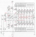
Vbe Q11 = 0.22V
Vbe Q10 = 0.23V
Vdc over R39 or R40 should be 4.0mA * 274 ohm = 1.096V, but reads ~ 1.3V already.
So, q10-q11 are closed but do run ~ 1.3/274 = 4.7mA both. Most curious.
...
Almost the same with Q8-Q9: 0.26V, but here is Q7 not fully operative yet.
...
Check Q10-Q11 thouroughly. CE swapped?
Vbe Q10 = 0.23V
Vdc over R39 or R40 should be 4.0mA * 274 ohm = 1.096V, but reads ~ 1.3V already.
So, q10-q11 are closed but do run ~ 1.3/274 = 4.7mA both. Most curious.
...
Almost the same with Q8-Q9: 0.26V, but here is Q7 not fully operative yet.
...
Check Q10-Q11 thouroughly. CE swapped?
Voltages are moving around making our job harder. An updated diagram is attached. I can't tell what is causing it.
DN2530 is a low threshold depletion-mode mosfet. It is what was in the amplifier when I got it and it does not appear to have been changed (it still has the manufacturer's markings).
I originally had R43 and R44 as 100-ohm resistors. I had meant to double them for 50-ohms but forgot. In any case, it makes no difference whether there are resistors from 10 to 100 ohms or the original Schottky diodes at R43 and R44. Voltage at output transistor base remains the same to within hundredths of volts.
Q8, Q9, Q10 and Q11 appear correct. They are correctly oriented in the circuit and still have the manufacturer's original markings. They are responsive to changes in voltage at the base induced by changing the value of R35.
Each integrated diode shows a voltage drop and none appear to be open. Voltages at each integrated diode are listed on the diagram for the first test condition with the 100-ohm resistors at R43 and R44.
VB at Q10 and Q11 seems to track rail voltage.
Attachments

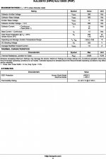
It seems it would be helpful to do some testing at a higher rail voltage. I have been staying near the 20mV specified bias across the 0.2-ohm resistors because I want to avoid damaging anything, especially the matched output transistors. The NJL3281D/NJL1302D appear, however, to be rated for 15 amps continuous collector current (datasheet below). 20mV represents only one-tenth of an amp, so it seems I could turn the rail voltage up rather more.
How much continuous current should I be comfortable running through each of these output transistors?
Thank you!
How much continuous current should I be comfortable running through each of these output transistors?
Thank you!
Attachments
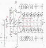
In all supplied pictures Q5 has remarkable higher Vbe then Q6, where approx the same is expected. Q5-Q6 are connected to the bias-legs. Check Q5.
We're now shooting at random, but odd is it, so all and everything is target...
We're now shooting at random, but odd is it, so all and everything is target...
Mosfet Q7 is suspicious, voltage across R35 shows gate current leak. Seems drain current of Q7 should be < 1mA, unlikely a DN2530, perhaps an LND150?
Last edited:
Now we are getting somewhere. Q8 and Q9 were in saturation. Changes to voltage at the base were changing current in R33 and R34 and having a little effect on voltage at the emitter, but not because the transistors were active. Replacing Q7 with a potentiometer now allows actual control over the bias, which I have not had until now. I had substituted out Q7 earlier, but I had not replaced Q5 and Q6 at the time and they were probably bad. I will do more testing today. Then maybe we can consider what is best for the bias circuit.
Soldering small mosfets is tricky, some gates are really fragile. Try shorting all 3 leads during soldering.
Ok, looked up to the DN2530 datasheet. Way to large current-transfer. Not a proper substitute from the original. Above serious supply flowing tens / hundreds of mA's. Should be a 1-10 mA range type instead. With normal pot back into control.
Find a proper sub for "1041". 2SK1041??? Specs? &c &c.
The DN2530 is the killer. And not original.
Find a proper sub for "1041". 2SK1041??? Specs? &c &c.
The DN2530 is the killer. And not original.
presuming everyone enjoys on engaging on search exercises as an uneccessary loop instead of serving the desired knowledge immediately
availability? pin config substitution?
no matter, i sent a pm already
availability? pin config substitution?
no matter, i sent a pm already
Q7 "1041" is a mystery. I find no such part in web searches. Only a JFET, not a (enhancement mode) MOSFET will work in this position, except that no JFET is good for 130VDC. If you use a typical MOSFET here, it is biased completely off and no current will be conducted by Q8 and Q9, but we seem to have too much current so that's not the problem. Never the less the problem may be related to Q7.
I assume you realise this amp has no gain. It is simply 4 stages of Emitter follower. There are other dubious design features but at least you provided a schematic. Problems like this are usually caused by wiring mistakes and bad assumptions.
I assume you realise this amp has no gain. It is simply 4 stages of Emitter follower. There are other dubious design features but at least you provided a schematic. Problems like this are usually caused by wiring mistakes and bad assumptions.
Last edited:
- Home
- Amplifiers
- Solid State
- Help with transistor amplifier output stage?