marce said:
The speakers return signal wants to be located as near to the
PSU caps ground pins as possible, the only other output related
current then C12 ground pin, this could be
isolated from the ground plane and returned to the same point
as the speaker return by a wire link.
The ground plane would then not have any large currents running
around, and the numerous benefits of the ground plane can be realised.
Welcome aboard, Marc!
I have used some of your suggestions, hopefully to good effect.Let me know if you think I'm getting closer to a good layout.
PB2 said:
Those large caps have relatively large ESL and therefore the bit of extra trace is really insignificant in comparision. You are on the right track asking does it really matter,
What is critical is the small HF bypass caps near the output transistors, and you do have those close.
You might find this interesting, note their ultra low distortion, however the complexity is high:
http://home.tiscali.nl/audio/Wiring.html
Hi Pete,
I have been looking at the power supply traces the same way, normally they are wires hovering somewhere above the board. The advantage in that is the ability to move these wires around if a problem is apparent.
That I have them well away from the input stage should make a difference.
Yes, I have checked out the new amp,. It is quite complicated, that's true. Does the extra complexity and lowered distortion make an audible difference though? Maybe not, but a fine job all the same.
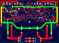
Further refinements. Added extra pads to the supply caps to give some more flexibility for parts selection. Bulked up the traces to the supply caps from the bridge and rearranged things a bit better.
I'm toying with the idea of a ground plane on the power supply side of the board, connected to the high current ground. Does this have any possible benefit?
I'm toying with the idea of a ground plane on the power supply side of the board, connected to the high current ground. Does this have any possible benefit?
Attachments
It's looking good John, nice work!
Where you really want the power ground plane is along the power transistors to provide a low inductance path between the HF bypass caps, the main speaker output, and the zobel. The output transistors are HF devices that can oscillate, the large PSU caps are not. It would not hurt to fill near the large caps just to have a low resistance path and perhaps reduce the fields around the bridge diodes. I would cut the output ground between the large caps and join it with a plane along the output devices. Connect the input plane to the output ground at the speaker output which is the star point. The diff amp needs this point as a reference for it to correctly reference the output. A zero ohm resistor could be used here if you are worried about hum loops, however I doubt that you'll have a problem.
I would move the input stage bypass cap ground connections to the input ground plane, this is important to provide a short HF path.
Did you consider moving the fuses down and the caps up, will make it easier to access the fuses.
Pete B.
PB2 said:
Where you really want the power ground plane is along the power transistors to provide a low inductance path between the HF bypass caps, the main speaker output, and the zobel.
I would move the input stage bypass cap ground connections to the input ground plane, this is important to provide a short HF path.
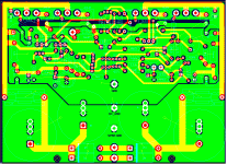
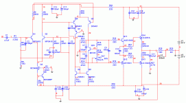
I have added the ground plane at the outputs and around the supply caps. I've also changed the bypass cap ground to the main ground.
The ground scheme now is this:
Attached to the high current ground are the power supply caps, output stage bypass caps, zobel and the decoupling caps.
On the main ground are the input stage bypass caps and all of the other low current grounds including R32 - the 10 ohm connection to the signal ground trace.
I see both of these ground planes being attached to a central ground on the chassis. Speaker return ground will connect directly to the high current ground on the board, near the PS caps.
Here's how it looks:
Attachments
Hi MJL,
What type of rectifier diodes are you planning to use?
I would suggest you to use 6A/200V types, say P600D.
On the margin I prefer these metal-cased 25A/200V, or even 35A bridges, mounted on the case. I've never used single 1N540X, P600X, etc. diode types for >100W amplifier projects.
Once I saw the inner of a 180W/8Ohm strereo amp that used four 1N5404s in graetz configuration wizhout any problem. These 1N540X diodes are really workhorses.
Best regards,
PS. It's nice to see a new amp design borning. Keep posting! 😎
Donk said:
What type of rectifier diodes are you planning to use?
I would suggest you to use 6A/200V types, say P600D.
Hi Donk,
They are 1N5406. These are 3A, 600V.
Once again, these are what I have on hand, so if there is a better choice, let me know. The P600D is only available through Digikey in a bulk amount (1000 units).
Thanks for the words of encouragement. Like I said earlier, I'm not trying to break new ground here, just to end up with a good performing amp that will run on the higher voltage. It's also been fun and educational to do it this way.
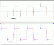
I have spent the afternoon testing the simulated amp (I dub it "Patchwork") and comparing it to the simulation of the SymAsym.
First I thing I did was to compare the signals on the inputs of the differential pair, to see if they match. For patchwork the sine wave comparison showed no difference, so I switched to squarewave. It shows a big overshoot on the leading edge of the inverting input (from feedback). To see if this was way off the chart as far as performance goes, I tested the symasym.
The results are below. Each is running a 20KHz squarewave at about 1/3 power output. There are two traces on each screen, each a different colour for A and B channels on the virtual oscilloscope.
My question is what is causing this overshoot? Is it normal or is there a way to reduce it? Will reducing it make a audible difference or is this just a stability concern?
Ideas? Comments?
Attachments
MJL21193 said:I have spent the afternoon testing the simulated amp (I dub it "Patchwork") and comparing it to the simulation of the SymAsym.
First I thing I did was to compare the signals on the inputs of the differential pair, to see if they match. For patchwork the sine wave comparison showed no difference, so I switched to squarewave. It shows a big overshoot on the leading edge of the inverting input (from feedback). To see if this was way off the chart as far as performance goes, I tested the symasym.
The results are below. Each is running a 20KHz squarewave at about 1/3 power output. There are two traces on each screen, each a different colour for A and B channels on the virtual oscilloscope.
My question is what is causing this overshoot? Is it normal or is there a way to reduce it? Will reducing it make a audible difference or is this just a stability concern?
Ideas? Comments?
As I explained somewhere in the middle of the thread, some crusial resistors are missing and also one or two transistors would find their place in schematics. BTW the Bryston output stage would be much better for your application. BR 😉
Hi Lazy Cat,
Have you seen the latest schematic? It's stuffed with resistors! Look on post #202 for the latest update.
The Byston output stage is not as good as this EF, at least not on the sim. If it would fix the overshoot, I don't know.
A better option for the output stage is the CFP, which I tried but abandoned for this design. I am working on a high power class B amp that will use the CFP output. Shown below, when tested on the differential inputs, it showed no overshoot. The only difference is the classB topology and the output stage. I don't think it was the class B that made the difference, so it must be the output stage.
Here's the output stage for the class B I'm working on:
Attachments
Hi again,
even though this is not a high speed board, signal integraty is paramount.
I still strongly disagree with the ground scheme as shown, you have 3 isolated grounds joined by a tiny track, which is borderline for the current. You could effectively draw it out as 3 gounds joined by an inductor, the high current grounds are joined by that little track, high inductance, which I would suspect during bass transients would cause that ground plane to rise in voltage, causing a difference in ground potential. The base drive for the op transistors crosses a split in the ground plane, not good.
Now I know its not a high speed design, but in my opinion it dose not matter what if any clocks speeds are involved, signal integraty and EMC compliance are paramount (now I'm repeating myself, old age and poverty).
I would also say the pos supply tracks are a bit thin, I would use the figures for a 10 deg temp rise, and where possible use copper pours for pos supply (again low inductance) approx 250 thou wide track for 15A.
MJL21193 said:
My question is what is causing this overshoot? Is it normal or is there a way to reduce it? Will reducing it make a audible difference or is this just a stability concern?
Ideas? Comments?
The overshoot is completely "normal", the feedback just has much work to do...
Your sims of symasym do not match mine, there should not be that much ringing. In your sims symasym is unstable.
Mike
marce said:Hi again,
even though this is not a high speed board, signal integraty is paramount.
I still strongly disagree with the ground scheme as shown, you have 3 isolated grounds joined by a tiny track, which is borderline for the current. You could effectively draw it out as 3 gounds joined by an inductor, the high current grounds are joined by that little track, high inductance, which I would suspect during bass transients would cause that ground plane to rise in voltage, causing a difference in ground potential. The base drive for the op transistors crosses a split in the ground plane, not good.
Now I know its not a high speed design, but in my opinion it dose not matter what if any clocks speeds are involved, signal integraty and EMC compliance are paramount (now I'm repeating myself, old age and poverty).
I would also say the pos supply tracks are a bit thin, I would use the figures for a 10 deg temp rise, and where possible use copper pours for pos supply (again low inductance) approx 250 thou wide track for 15A.
Hi,
Yes, agree with you marce. As is there is at least one completed inductor (loop) between decoupling caps on top of board and supply ground, low level circuitry is surrounded by that "coil".
My liking is as suggested earlier a very small area power ground.
But MJL may have settled on his PCB design and we must respect that.
marce said:
I still strongly disagree with the ground scheme as shown, you have 3 isolated grounds joined by a tiny track
Hi Marc,
I thought that by separating the grounds, I'd wind up with a cleaner front end. If this will cause more problems than it will solve, I'm willing to change.
In my active amp thread here:
http://www.diyaudio.com/forums/showthread.php?s=&threadid=104118&perpage=25&pagenumber=3
I did a similar type ground scheme, with the filter and buffer stages separate from the high current from the chip amp. I have no completed that project, as I have pretty much stalled out due to a problem detailed in the thread. I do have one channel complete (three active amps) and the performance is very good.
This patchwork amp is a different layout, with higher currents involved and the added complication of power supply on board.
I can redo anything on the layout, as there is nothing written in stone about it, though I do favour the overall component placement.
MJL21193 said:
Hi Marc,
I thought that by separating the grounds, I'd wind up with a cleaner front end. If this will cause more problems than it will solve, I'm willing to change.
In my active amp thread here:
http://www.diyaudio.com/forums/showthread.php?s=&threadid=104118&perpage=25&pagenumber=3
I did a similar type ground scheme, with the filter and buffer stages separate from the high current from the chip amp. I have no completed that project, as I have pretty much stalled out due to a problem detailed in the thread. I do have one channel complete (three active amps) and the performance is very good.
This patchwork amp is a different layout, with higher currents involved and the added complication of power supply on board.
I can redo anything on the layout, as there is nothing written in stone about it, though I do favour the overall component placement.
John,
You need to think about current flow.
Consider how few grounds there are in the front end, and in the output/power side. A star solution is simple when there are so few connections, just place them very close together and then not only do you have a star but one with short paths. This is why you want the power grounds all at the output side, with gound paths to the caps simply to connect them in essentially a star arrangement to the output side.
The input also has few grounds, consider that most op amps have no gound connections to the package, these too should be close and then again the plane just acts as a shield for the rest of the circuitry. The job of the diff amp is to compare the output to the input, and your input ground should connect at one point to the "star" of your output circuit in order to sample the output signal at the correct point. It is like a sense line in a power supply.
It's really not that complicated, however things can go very wrong.
Pete B.
MikeB said:
The overshoot is completely "normal", the feedback just has much work to do...
Your sims of symasym do not match mine, there should not be that much ringing. In your sims symasym is unstable.
Mike
Thanks for the info on the overshoot.
I modeled your amp according to the schematic, and I will post the simmed schematic here. I checked it over several times for some of my bone-headed mistakes, but I see none.
The model is running on the same program as the one in this thread. Like I've said before, I have modeled a few amps with this simulator, including the Krell KSA50, the Bryston 3B, the Rod Elliot project 3A, the DX amp (first version). Of all of these, the Symasym ran the smoothest.
As for the ringing at 20KHz, I have no idea why it would be there in the sim. Do you have any ideas as to why this would be the case? A faulty model perhaps? Pete (PB2) has told of bad models, especially On-Semi's.
Attachments
4fun said:
But MJL may have settled on his PCB design and we must respect that.
Hi 4fun,
I don't have my mind made up on the layout yet, though I have put a considerable amount of time into the present configuration.
My hopes are to be able to change the ground scheme without a major overhaul of the component layout.
I would be willing to move the PS parts, but I'd prefer to leave the "core" as is.
MJL21193 said:
As for the ringing at 20KHz, I have no idea why it would be there in the sim. Do you have any ideas as to why this would be the case? A faulty model perhaps? Pete (PB2) has told of bad models, especially On-Semi's.
The mjl3281 model from onsemi is useless bad. Try the mjw0281/0302 models, they work very fine.
Mike
Hi Mj,
are q7 base and r13/14 connected to the correct ground?
Which ground should the relatively clean c13/14/16/17 be connected to?
Where should r3 connect to?
are q7 base and r13/14 connected to the correct ground?
Which ground should the relatively clean c13/14/16/17 be connected to?
Where should r3 connect to?
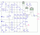
Hi Again,
the example below will hopefuly illustrate my ramblings on ground schemes, and I hope help give ideas for future designs, if not this one, though I think with a bit of tweeking of component placement a similar idea can be implemented.
The ground scheme illustrated is the one on the left, it effectively a star ground but with low inductance planes rather than tracks.
(When you start throwing surface mount components on a board it is very very hard to do traditional star grounding dure to component sizes etc). the three legs of the ground plane correspond from left to right as follows.
The star point is the big electroylitic at the top. The left hand leg has a bridge rectifier and so this leg has the 50Hz crud running round it. The middle leg is a high current 350V switching at 100KHz Iductive load, so all that noise is in that leg, the last leg is all the controll circuitry, so thats a nice clean leg. Though not audio I thought it the best example of what I am getting at.
When laying out this and similar PCB's I tend to sort the components into the various stages (output, input, control etc) and look at them in terms of power requirments first, as if you aint got clean power you are gonna have trouble.
Would also recomemd bypassing the rectifier diodes with 0.1uf or similar as these can be noisy when switching and at 50/60Hzs it can be quite an intrusive noise.
Dinner time over see you tomorrow Chaps.🙂
Attachments

- Status
- Not open for further replies.
- Home
- Amplifiers
- Solid State
- Help with this amp? A patchwork product of simulation