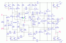
MikeB said:Hmm, i think you will blow up c15!
Mike
Thanks for pointing that out Mike. I have been working with 3 or 4 saved versions of this schematic, and the one posted has that cap reversed (somehow, it got reversed).
So much for the "final schematic update".😱
Otherwise Mike, how does it look?
Here it is again, fixed:
Attachments
Hi John,
Nice progress, did you consider putting main power and ground on the top plane?
Pete B.
Nice progress, did you consider putting main power and ground on the top plane?
Pete B.
Hi john,
Yes, looks better.
How about running both rails on one side of the board. You could use opposite layer to jump over to "the otherside" on top of the board. This should minimise the magnetic fields and inductance as the loops will be very small. As is the whole board is surrounded by high currents and corresponding magnetic fields.
Look at commercial amplifiers, you almost never see the rails wrapped around the circuit.
Thoughts?
Yes 4fun, I was having similar thoughts, however what I'm more concerned about is that if the output ground is taken near the output transistors, then there will be large currents through the ground plane to the supply caps. Even if the output ground is moved close to the caps, the output RC network provides a path for current in the ground plane at HF.
One solution, I think, and I've not put a lot of thought into this, is to move the caps close to the outputs, and the driver circuitry away. This is rather extreme and a major change.
Another solution would be to run wide power lands on the top, with a matching wide ground path on the bottom, for each main power trace. Then isolate the ground plane from these high current traces where it acts as the quiet front end ground.
Having the .1 uF bypass caps close to the outputs, with a close return path to the output ground will provide a short path for the HF loop. The simple theory here is to isolate the input ground plane so that it is impossible for high currents to flow through it. This is why I suggested isolating the grounds at the start, the front end ground would then be connected at one point to the output ground. I'm thinking that the transformer center tap, and speaker output ground point should be close to the output transistors. The caps then just have a bit of wide trace connecting them to the output stage. Hope this makes sense.
I'd say that you can drop C3 and C18 wouldn't hurt to put a .1 uF near each output transistor, to ground.
Also, John, don't remember if I mentioned, but the current mirror pair can be low voltage/current high beta types.
The large cap on the Vbe multiplier that I questioned, is to minimize signal current induced bias modulation. I'd have to simulate to see if this is a real issue.
Pete B.
Just to add: I"m aware that isolated planes are often not suggested, but this is really just the path for the large caps, and it is not a 500 MHz radio design.
PB2 said:Hi John,
Nice progress, did you consider putting main power and ground on the top plane?
I'm open to suggestions. How much of a difference will this make?
Would another possibility be to mirror the power traces on both layers? Truly, these are well away from the "heart" of the circuit.
PB2 said:
...however what I'm more concerned about is that if the output ground is taken near the output transistors, then there will be large currents through the ground plane to the supply caps.
I'd say that you can drop C3 and C18 wouldn't hurt to put a .1 uF near each output transistor, to ground.
I take speaker output ground directly from the chassis star ground. The layout as it stands now has one main ground lead to star ground with the input ground isolated from the main board ground with a 10 ohm resistor.
I have C4 and C19 right next to the outputs which are .1uF. Did you mean that I should double these?
4fun said:Hi john,
Yes, looks better.
How about running both rails on one side of the board. You could use opposite layer to jump over to "the otherside" on top of the board. This should minimise the magnetic fields and inductance as the loops will be very small. As is the whole board is surrounded by high currents and corresponding magnetic fields.
Look at commercial amplifiers, you almost never see the rails wrapped around the circuit.
Thoughts?
Hi 4fun,
I had a look at this as posted by PB2:
http://www.diyaudio.com/forums/attachment.php?s=&postid=614697&stamp=1112913063
It's the KSA50 clone that has the rails to the outside of the board. I though I could avoid a long run across the board, as I had it before. I know it's strictly not a good idea to create a modulated magnetic field around a circuit, but how bad are the effects? Are they minimized by, as I mentioned above, mirroring the rail trace on both layers?
Are the problems introduced by a poured ground plane (parasitic capacitance, inductance) out weighted by the good it will do?
PB2,
I agree.
My sugesstion as follows:
Move the supplycaps as far up in the corner as possible, arrange so the closest cap in the corner supplies to the far end and vice versa. Ground "plane" betwen caps will be the power ground to where speaker return, possibly other "power" decoupling and output zobel network connects. And from here one narrow connection path to a low level ground plane.
MJL talked about separate power and signal grounds in the beginning.
Edit: Were typing while you posted MJL.
Edit2: Has to sleep, late here in the north.
4fun said:PB2,
I agree.
My sugesstion as follows:
Move the supplycaps as far up in the corner as possible,
Hi,
Is there any way you could sketch what you are proposing? I'm not sure if you mean to put the PS filter caps closer to the output transistors?
MJL21193 said:
Hi,
Is there any way you could sketch what you are proposing? I'm not sure if you mean to put the PS filter caps closer to the output transistors?
Hi,
I might be able to do a sketch in some time.
Yes, I mean to have as short and compact power traces as possible.
Yes, if PS filter caps are placed on the main pcb, they should be close to output transistors.
I know my suggestions may seem unnecessary but I do beleave that the pcb layout has great importance, at least for the performance in the top end frequencies.
MJL21193 said:
I'm open to suggestions. How much of a difference will this make?
Would another possibility be to mirror the power traces on both layers? Truly, these are well away from the "heart" of the circuit.
I take speaker output ground directly from the chassis star ground. The layout as it stands now has one main ground lead to star ground with the input ground isolated from the main board ground with a 10 ohm resistor.
I have C4 and C19 right next to the outputs which are .1uF. Did you mean that I should double these?
The chassis ground should simply connect to protective ground from the plug, and act as a shield, see here how it is somewhat isolated from the amp signal ground:
http://sound.westhost.com/project04.htm
This is sometimes required because house wiring protective ground is not always clean.
The chassis should just serve as a shield, it seems to me that your grounds are fully covered by your PCB. I expect that your input and output jack grounds will be isolated, so just run grounds from your PCB to each one. Your PCB ground is the star ground. Then run a wire from your PCB to chassis ground where the green line cord wire connects. Some use a 2 to 10 ohm resistor between signal and chassis ground so that very high currents cannot flow through the ground paths.
Pete B.
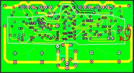
I've marked up your layout in the attached image showing how I'd cut the plane to isolate the front end. You could clean up the large power traces to make them look nice. I did this quickly and you might want to optimize it a bit near the output stage.
Pete B.
Pete B.
Attachments
Hi, my first post on this paticular thread that I've been following.
Hi PB2, I would like to disaagree with your solution above,
it you are going to cut the ground plane so much you negate its
benefits and mite as well go back to star grounding traces.
The speakers return sinnal wants to be located as near to the
PSU caps ground pins as possible, the only other output related
current then C12 ground pin, this could be
isolated from the ground plane and returned to the same point
as the speaker return by a wire link.
The ground plane would then not have any large currents running
around, and the numerous benefits of the ground plane can be realised.
The magnetic interefence etc are on board EMC issues and these are
best sorted at source by a ground plane.
If the ground is left contigous then slots may be cut in it at a later
date if any interefrence is encounted, its easier to mod a board this
way than trying to bridge slots.
BTW this is only my humble (bumble!) opinion.
You are welcome to your opinion, and I disagree.
You want a quiet plane for the front end.
Planes or star can both be made to work just fine for audio.
John chose planes so I'm just trying to help.
Here's another example John, might get some layout ideas:
http://home.tiscali.nl/audio/OP-stage.html
You should also consider having the rectifiers so close to the
front end, the current loop is short and just to the caps so it
might not be an issue but keep it in mind. You could always
move the bridge to the chassis if is is a real issue, I do prefer
it on the PCB for wiring simplicity.
Pete B.
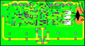
Hi,
I did a simple (ugly) MS paint sketch that shows my suggestion for placing caps and rails. "Small Signal Ground" could be a plane..
Marce, I agree, a disrupted groundplane creates loops, no good IMO.
Is there any way you could sketch what you are proposing
I did a simple (ugly) MS paint sketch that shows my suggestion for placing caps and rails. "Small Signal Ground" could be a plane..
Marce, I agree, a disrupted groundplane creates loops, no good IMO.
Attachments
I've been quite busy with work for the past few days, so I'll need a bit of catch-up time.
I'm trying to find time over the weekend to redo the layout, putting some of the suggestions to use. I am also going to start to prototype the circuit on the breadboard to see how it runs. I know, I've said that before, but this time I mean it. 🙂
I've now decided that I want this amp to be as good as it can be. Buying new parts, refining the circuit to the point where I can't see room for much improvement, optimizing the PC board layout - all of this effort should be rewarded with an exceptional amp.
I have ordered the 2SA1011's from Ampslab but they haven't arrived yet. I'm still compiling an order for Digikey, they ship by courier, so I'd have those parts in a couple of days. The critical items from there are the LM394's.
With that said, I should be good to start prototyping with the parts I have to determine stability and to get a rough idea of the performance.
Hi John,
Let me offer this, the only long traces going around your board are connections to the large PSU caps. These are often connected by long wires in many designs, your PC traces are relatively shorter. One way to think of this is that what I left with the ground plane is the amp, and the outer traces as the power supply. Those large caps have relatively large ESL and therefore the bit of extra trace is really insignificant in comparision. You are on the right track asking does it really matter, no taking out an inch of trace might matter if this was a 500 MHz radio, not for the large caps at audio frequencies. What is critical is the small HF bypass caps near the output transistors, and you do have those close.
You might find this interesting, note their ultra low distortion, however the complexity is high:
http://home.tiscali.nl/audio/Wiring.html
Pete B.
Ok.
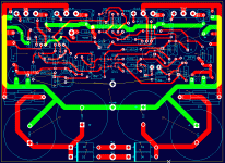
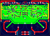
I've worked for a considerable time on the layout and have come up with, what I think, is a major improvement. Biggest change is a new high current ground that is separate from the main board ground and the signal ground.
I have moved a lot of components, to reduce trace length and to optimize routing. I have pushed the electrolytics away from the heatsink area and moved the emitter resistors on the output stage closer to the heatsink.
The input stage is almost dead centre of the board now, well away from potential interference.
I think I'm getting closer. Anyhow, have a look:
Attachments
- Status
- Not open for further replies.
- Home
- Amplifiers
- Solid State
- Help with this amp? A patchwork product of simulation