

MJL21193 said:I am getting to the board layout point on this, so if there are any obvious defects or other suggestions, now would be the time to let me know.
Please look it over and help a rookie out.🙂
I suggest that you implement Bryston type of current output stage. In that case driver transistor flows only one base current to both output transistors, have half dynamic thermal dissipation and therefore acts more easily with less distortion. Because of that solution you'll better use 22 ohm base-emmiter resistor at output transistors instead of 50 ohms, so driver will have double quinscent current without problem. 😉
Lazy Cat said:
I suggest that you implement Bryston type of current output stage.
Hi Lazy Cat,
I tried the Bryston output earlier on the class B, and have just tried it on this one. I found (in the simulation) that high frequency distortion was higher. Also, to maintain output current sharing between both pairs of output devices, the collector resistor on the driver would have a value of ~55 ohms (reducing quiescent current).
I think I will stick with the straight EF, as it seems to give the best results.
MJL21193 said:
Hi Lazy Cat,
I tried the Bryston output earlier on the class B, and have just tried it on this one. I found (in the simulation) that high frequency distortion was higher. Also, to maintain output current sharing between both pairs of output devices, the collector resistor on the driver would have a value of ~55 ohms (reducing quiescent current).
I think I will stick with the straight EF, as it seems to give the best results.
The small difference between collector and emitter resistors is normal if you want exactly the same bias current (difference appears because the driver base current adding the small amount of voltage to emitter resistor) through output pair. After you calibrate the resistors properly than there will be no problem in dynamic conditions. In practice it's clearly obvious and confirmed that this solution sounding much better than simple EF output stage.
And you can always use 22 ohms collector-emitter resistors to give you app. 25 mA driver bias current.🙂
Hi John,
Been meaning to comment, looks good, the LM394 is available in a plastic DIP that might be less expensive. Not sure if you lifted the requirement to use what you have for transistors, but you might want to consider a better VAS if so. Remember that it has to have high current capability to handle the even brief short circuit condition. Consider a short where the input signal is large enough to cause max peak current, but too small to blow the fuse.
I like a servo to eliminate the big feedback cap, but you need a supply for the OP amp which is a bit of a pain.
Pete B.
PB2 said:
Not sure if you lifted the requirement to use what you have for transistors, but you might want to consider a better VAS if so. Remember that it has to have high current capability to handle the even brief short circuit condition.
Hi Pete,
Yes, I have lifted the new parts ban. Any suggestions for the VAS? I'm not sure why the MJE15031 is a bad choice.
The LM394 is only available to me (via Digikey.ca - the only supply I'll deal with now) in the TO-5 package. The price is fine, as I only need two of these, I'll gladly spend that for better quality.
The problem I have, is I don't have either a spice model or a proper footprint for Ultiboard for layout. I made a rough symbol layout for schematic (as seen above). For the board layout, I put two TO=92 back to back, changing the pin locations.
I need to order the LM394's and a few other parts for future projects. In the meantime, I will start to prototype this on the breadboard this weekend, using two BC550 instead of the LM394.
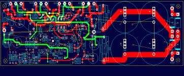
I have also been busy doing a tentative board layout. As pictured below, it is 191mm x 62mm and includes all power supply components. One of the things I learned recently, is to give myself a little more space on the board, not to pack it in so tight. Still, I have managed a fairly compact design.
On this layout, I have the Vbe multiplier transistor sharing a small heatsink with the VAS and drivers. Is this ok for thermal tracking?
Attachments
Hi MJL21193,
Regarding layout:
How about running the (-) rail trace that supply the power transistors on the top board edge. Then you will have much less magnetic fields affecting lower level stages.
And of course beefier rail traces, but I guess that you are early in design and just laying out traces for later fine tuning.
Thoughts?
4fun said:Hi MJL21193,
Regarding layout:
How about running the (-) rail trace that supply the power transistors on the top board edge.
Hi 4fun,
I have the output transistors on the edge of the board, mounted vertical. This doesn't leave any room. If I move them inwards, it will be a problem for mounting on the heatsink. Besides, not much of it is close to small signal area.
I consider this layout close to being final. I'm looking for suggestions, such as yours, to improve it.
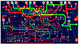
I have a better pic below, showing the "business" section only. Note that power ground throughout the board is not connected, as I'll do a poured ground plain on the top (green)
Attachments
Hi,
the cost of the lm394s will pay for ALL the other transistors except the outputs. That decision has doubled the semi costs.
The VAS should be a low Cob type with adequate Vce0 and probably a medium power type with 50 to 150mA Ic and fT>100MHz. I use 2sa1360/c3423, but there are many others.
I use the same for the pre-drivers, if fitted.
I only use driver transistors in the driver locations.
I just measured the gain of a single sample MJE15035.
DMM said hFE=178. but from 1mA (186) to 25mA (205) the gain exceeded what dmm said. I am amazed that a 50W 4A device has this much gain and so close to linear over that range of Ic.
I tried measuring at 500uA and 200uA but readings are becoming less accurate down at these Ic levels and gain is certainly starting to fall. Looks like DMM is using a fixed base current of around 1uA.
I wish I had a 15031 to measure.
MJL21193 said:On this layout, I have the Vbe multiplier transistor sharing a small heatsink with the VAS and drivers. Is this ok for thermal tracking?
With EF output topogoly the Vbe should be mounted with the output transistors, not the drivers. You have decided on EF?
regards
MJL21193 said:
Hi 4fun,
I have the output transistors on the edge of the board, mounted vertical. This doesn't leave any room. If I move them inwards, it will be a problem for mounting on the heatsink. Besides, not much of it is close to small signal area.
Yes, current power traces is fairly away from low levels. I can alo spot short path for the power ground and hopefully no small signal areas surrounded by high current ground traces. 😉
MJL21193 said:
Hi Pete,
Yes, I have lifted the new parts ban. Any suggestions for the VAS? I'm not sure why the MJE15031 is a bad choice.
The LM394 is only available to me (via Digikey.ca - the only supply I'll deal with now) in the TO-5 package. The price is fine, as I only need two of these, I'll gladly spend that for better quality.
The problem I have, is I don't have either a spice model or a proper footprint for Ultiboard for layout. I made a rough symbol layout for schematic (as seen above). For the board layout, I put two TO=92 back to back, changing the pin locations.
I need to order the LM394's and a few other parts for future projects. In the meantime, I will start to prototype this on the breadboard this weekend, using two BC550 instead of the LM394.
I have also been busy doing a tentative board layout. As pictured below, it is 191mm x 62mm and includes all power supply components. One of the things I learned recently, is to give myself a little more space on the board, not to pack it in so tight. Still, I have managed a fairly compact design.
On this layout, I have the Vbe multiplier transistor sharing a small heatsink with the VAS and drivers. Is this ok for thermal tracking?
Hi John,
I suggest that you download the .pdf data sheet for the MJE15031, and the MJE15035 and look at them side by side. They seem to be very similar from the basic specs, however take a look at the hfe, and where they're optimized for best performance. The 031 is best around 500 mA to 2A, however note the poor SOA performance at 50V, it will only handle about .5A. The 035 is best around 100 mA to 1A, is spec'ed down to 10 mA, and will handle about 1A at 50V obviously twice the power. Remember we raised the operating point to about 10 - 20 mA and we're not even close to the optimal range for the 031. These parts are much better than the older medium power transistors, having an Ft of 30 MHz and better beta characteristics.
There are many video output transistors that are have been mentioned here at diyAudio, however they typically have a max Ic of only 50 mA, a few with 200 mA which is far too low when only fuses are used for protection. You should look at adding a VAS protection transistor as was done in the Leach design if you wish to use any of these low max current devices.
I think that the MJE15035 is your best bet if you want to keep it simple, you might want to allow for a VAS protection transistor in your layout. The 035 is higher beta and I would add an emitter resistor also in your layout.
I think I suggested the 2N5550, forgot to mention that the 2N5551 has higher beta if you are buying new, 5550 is fine if you already have them.
I like film caps where ever possible in the main amp section. Stacked low ESL caps for the HF PS bypass.
I'd use a thermal cutout switch to protect during over temp.
Spread the outputs out if this works with your planned heat sink.
The critical HF layout is the small bypass cap going from the output device collectors to ground, try to keep the paths short.
I'd keep the input and output grounds independent.
Greg is right about the Vbe multiplier going on the heat sink. You want it as close as possible to one of the outputs.
Pete B.
Here is my very similar power amp design that I've been simulating, that you might want to take a look at. This not complete, stability should be looked at and a few more details. I'd probably use a DC Servo to eliminate the large feedback cap. I'd prefer a voltage reference in place of the LED, but LEDs are common readily available parts. Changed the FB resistor to match yours:
http://baselaudiolabs.googlepages.com/PTLB_POW1.JPG
What are you getting for distortion with your design?
Pete B.
http://baselaudiolabs.googlepages.com/PTLB_POW1.JPG
What are you getting for distortion with your design?
Pete B.
AndrewT said:
the cost of the lm394s will pay for ALL the other transistors except the outputs.
I just measured the gain of a single sample MJE15035.
DMM said hFE=178. but from 1mA (186) to 25mA (205) the gain exceeded what dmm said.
Hi Andrew,
When I bought the MJE15031's, it was because I could not locate MJE15035 - which was my first choice. That was more than 2 years ago. I will order a few of these.
The layout on the board for this LM394 is the same as two TO-92's back to front, so if someone else is foolish enough to use this design, it can accomidate the cheaper alternative.
Greg Erskine said:
With EF output topogoly the Vbe should be mounted with the output transistors, not the drivers. You have decided on EF?
Yes, EF for the output (written in stone). Thanks for that, I wasn't sure.
4fun said:
...short path for the power ground and hopefully no small signal areas surrounded by high current ground traces. 😉
What do you think of a poured ground plain on the top side of the board? Signal ground is seperate from power ground.
PB2 said:
Hi John,
I suggest that you download the .pdf data sheet for the MJE15031, and the MJE15035 and look at them side by side.
I think that the MJE15035 is your best bet if you want to keep it simple, I would add an emitter resistor also in your layout.
I like film caps where ever possible in the main amp section. Stacked low ESL caps for the HF PS bypass.
Thanks Pete,
After Andrew's post, I did look at the spec sheets for these. With my limited knowledge, I could see that the gain is higher. If it will be a more suitable candidate for the VAS, I'll order some. Is it worthwhile to use these for the drivers instead of the MJE15030/31? Keep in mind that I have about 8 pairs of these already.
I have all of the correct values in MKT caps. I also have some 100pF silver mica and 10pF, 22pF, 220pF and 100nF monolithic ceramics.
MJL21193 said:
What do you think of a poured ground plain on the top side of the board? Signal ground is seperate from power ground.
Hi,
Why not, as long as there is no serious interruptions (cutouts for other traces) from the shortest path where high current flows.
I think a true ground plane is more predictable (where there may only be holes for component leads)
In a ground plane that has interruptions there may be necessary to have some stub areas in order to prevent loops. I once experienced this when designing a 10-channel video amp (some ground trace cutting necessary)
I have limited experience of ground planes so I better stop here. 🙂
Some rambling: Let’s suppose we have two wide traces where high ripple current flows and we connect a decoupling cap to the edges somewhere along these traces. Now, how much current will go through the cap and how much will bypass it in these wide traces (that has some inevitable resistance)? I think we must make sure that as much current as possible goes through the cap (pad) and not around it, at least if we want just decoupling.
I will be interesting to se your futher progress and finally end result with possibly real life measurements.
PB2 said:Here is my very similar power amp design that I've been simulating, that you might want to take a look at. This not complete, stability should be looked at and a few more details. I'd probably use a DC Servo to eliminate the large feedback cap.
What are you getting for distortion with your design?
Yes, very similar. No Vbe transistor and a current source (sink?) on the diff input and VAS the only real differences. How does it run? The diodes across the differential pair (D6,D7) what do they do? I've seen that in a few designs, most notably the Byston ones.
I know little about servos, but they seem to be a complicated solution to avoid a cap or two in the signal path.
Distortion:
Output-------------------At 150 watts----------------At 4 watts
20Khz ----------------------0.048%---------------------0.017%
10Khz ----------------------0.017%---------------------0.006%
5Khz -----------------------0.008%---------------------0.003%
1Khz -----------------------0.003%---------------------0.001%
50Hz -----------------------0.002%---------------------0.000%
The distortion analyzer won't read at a higher resolution. There is a spectral analysis that's available in this simulator, and once I learn exactly how to set the output variables, I'll use that.
Still and all, the numbers above are about 20% better than the previous best performing design on this simulator (SymAsym).
Whether this is indicative of actual real world performance is anyones guess. I don't have a real distortion analyzer at my disposal. I do have a 400Mhz scope to give me a at least an idea of the performance.
MJL21193 said:
Yes, very similar. No Vbe transistor and a current source (sink?) on the diff input and VAS the only real differences. How does it run? The diodes across the differential pair (D6,D7) what do they do? I've seen that in a few designs, most notably the Byston ones.
I know little about servos, but they seem to be a complicated solution to avoid a cap or two in the signal path.
Distortion:
Output-------------------At 150 watts----------------At 4 watts
20Khz ----------------------0.048%---------------------0.017%
10Khz ----------------------0.017%---------------------0.006%
5Khz -----------------------0.008%---------------------0.003%
1Khz -----------------------0.003%---------------------0.001%
50Hz -----------------------0.002%---------------------0.000%
The distortion analyzer won't read at a higher resolution. There is a spectral analysis that's available in this simulator, and once I learn exactly how to set the output variables, I'll use that.
Still and all, the numbers above are about 20% better than the previous best performing design on this simulator (SymAsym).
Whether this is indicative of actual real world performance is anyones guess. I don't have a real distortion analyzer at my disposal. I do have a 400Mhz scope to give me a at least an idea of the performance.
Hi John,
The diodes across the diff pair are for protection, from say static discharge at the input or large overload signals. It is obviously not complete protection but it keeps the bases at nearly the same voltage so that there is not excessive Ib in either of the transistors. The input diff voltage is near zero in normal operation due to the high open loop gain, so they have no significant effect on normal signals.
I prefer current sources, and I've been meaning to mention that some claim that amps have large turn on thumps that do not use one on the diff pair, forgot to mention that earlier. The one on the VAS eliminates the large bootstrap cap. I perfer to eliminate electrolytic caps whenever possible.
Yes the servo is a pain, do whatever you're comfortable with.
The diode bias string is just that I was too lazy to get to a Vbe multiplier. If you're buying new outputs you might want to look into the thermal trak versions, which do provide diodes.
I did simulate with +/-56V supplies (no series R in the supply) and as I recall I got about .009% distortion at 20 KHz and 150W into 8 ohms. I had to sub some transitors simply because I believe that the On-Semi models are defective. I used Fairchild BD139/140 for the VAS and drivers, and andy_c's models for the outputs. The 139/140 would not work in real life, but seem to be good enough for this simulation.
Pete B.
no these drivers and most others have Cob~=30pF.MJL21193 said:........... If it (MJE1503x)will be a more suitable candidate for the VAS, I'll order some. Is it worthwhile to use these for the drivers instead of the MJE15030/31? Keep in mind that I have about 8 pairs of these already.
You should be looking at VAS and pre-drivers with Cob<=3pF.
The VAS (variable) capacitance pulls current out of and into the LTP. That is not nice.
Have a look at your MJE drivers. Measure the NPN & PNP gains. I have found a big mismatch between the NPN before and after going lead free (15034 vs 15034g). Maybe mine are rogue, but many are complimenting ONsemi's production prowess. Maybe I should order more samples to get a better match.
- Status
- Not open for further replies.
- Home
- Amplifiers
- Solid State
- Help with this amp? A patchwork product of simulation