Thanks for sending this great info, I checked the supply rail B 3 it’s marked 100v where the brown wire from power supply board is connected to the phono board , it’s on the phono board the 100v is marked . I have changed all the transistors on the “F” power amp board the all 2SC926A transistors changed to APT 124H or APT 127H transistors these were recommended by digikey parts specialist as it has the same ecb pinouts and better specs , the A705 transistors were replaced with BC 556B . I will take out the VFETS and see if I am able to adjust the bias . The way I changed the gate voltage to max reading was connecting the - black lead test wire of the fluke 189 digital meter on dc voltage setting to the speaker black ground terminal and the positive red test wire to the gate I was then able to adjust the max voltage via the bias adjust rt301 and rt351 vishay 2.2k 1/2w trimmers . The problem happen when you try to adjust the bias the way Sony mention the meter at mvdc setting and + lead of the meter to + terminal of speaker A the bias is not adjustable from 0.5mvdc with no input and volume turned all the way down . The C420 cap on the power amp board is 47uf/50 volt new nichicon KA SERIES cap . The other caps you mentioned are all 10uf/50v nichicon FG FINE GOLD series cap. All caps and transistors on the power amp board were replaced with better specs than original . I wish I am able to adjust the bias as this is the only item to take care of . The amp sounds awesome even without the bias being adjustable that is very strange to me! 🙂
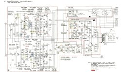
Hmm... after reviewing them I saw some errors.Attached some enhanced drawings for the 4650.
These are better & corrected.
In yellow are the differences between the original USA model and the later USA/E/AEP model mentioned in the service bulletins.
In blue the unmentioned and the recommendatios (C306/307 & C356/357).
I'm preparing an interconnection drawing (did that for the 5650 already), to clearify the various routings and (most important) the grounding plan.
Attachments
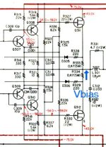
Something to do in a simulation!I will take out the VFETS and see if I am able to adjust the bias .
Just the vas-part, the bias and the drivers with that rail to rail totem pole.
That should give an estimate how the gate voltage varies with the bias setting.
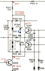
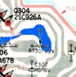
That's ok.The way I changed the gate voltage to max reading was connecting the black lead test wire ... to the speaker black ground terminal and the positive red test wire to the gate... - I was then able to adjust the max voltage via the bias adjust rt301 and rt35... trimmers .
See #20 "Sony_TA-4650_PowerAmp_Board_BIAS.jpg".The problem happen when you try to adjust the bias the way Sony mention... and + lead of the meter to + terminal of speaker A... - the bias is not adjustable... .
That's not referred to ground!
Thanks for all the diagram. Is there other way you can adjust the bias other than the Sony method . Both the left and right side bias cannot be adjusted the Sony service manual with black meter lead at test point on the power amp board for either channel ? Remember that the gate voltage can be adjusted if you put attach black meter test lead on the speaker negative terminal which is also the ground and positive lead of the meter to the VFET gate terminal. What might be the causes of bias not being adjusted for both channel . Thanks as always for your great help!👍😊
And the red at the positive speaker A output terminaland the speaker selector set on speaker A....with black meter lead at test point on the power amp board...
The bias current is measured over R334 (left ch). Not referred to ground!
Attachments
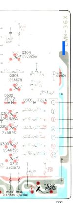
Only in case speaker A is selected. Not with the speakers off, not with speakers B selected; with speakers A + B selected, they're put in series with B on top of A.if you put attach black meter test lead on the speaker negative terminal which is also the ground
Use a proper ground, the chassis suffice.
Make sure the bias pot is operating as a variable resister, not a potentiometer!What might be the causes of bias not being adjusted for both channel
Attachments
Nope.Is there other way you can adjust the bias other than the Sony method .
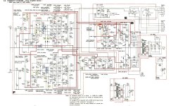
As I made a interconnect drawing for the two (or three?) variations of the 5650 amp, I've made one for the 4650 too (power amp, supply & output terminals).
My main concern is the routing of the supplies and the grounding.
Notice that a lot of (small) dc ground currents from the various boards are routed through the signal cables from the rear side back to the supply board, or through the chassis. The power amplifier board has three separated ground paths!
Attachments
Make sure the bias pot is operating as a variable resister, not a potentiometer!
Hi citizen, hope you are fine , I was researching setting bias and I came across a old post by of the knowledgeable VFET member he is proposing a different method of measuring the bias via case of a VFET how do you connect you fluke digital meter on mvdc scale to measure bias this way ? I have made a snap shop of his post and attached here . Your kind help as always is greatly appreciated ! Wishing you very happy holidays and a very happy new year! 👍😊
Attachments
Good idea: the drains are connected to the output with the 0.47Ω resistors. So instead measuring over one of the two 0.47Ω resistors, the reading will be twice the expected value.
Keep in mind that in normal conditions the speaker selector must be in position A. The A+B option connects the outputs A and B in series, with B on top of A.
If the output relay is broken or the contacts unreliable, no good bias measurement is possible.
MC&HNY
Keep in mind that in normal conditions the speaker selector must be in position A. The A+B option connects the outputs A and B in series, with B on top of A.
If the output relay is broken or the contacts unreliable, no good bias measurement is possible.
MC&HNY

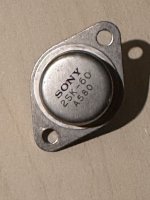
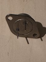
how do you connect the + - leads of the digital meter to measure drain of the two 2sj18 and 2sk60, do you connect the negative lead of the digital meter to the out er case which also drain of the VFET say negative lead on case of VFET 2sk60 and the positive lead to the the case of the other VFET 2sj18 ?!
These Sony V-fet amplifiers ('4650' and '5650') are the only two solid state amplifiers ever produced with a drain-to-drain output, as the V-fets are the only solid state devices in both polarities which operates as triode vacuum tubes. (The Wega 4810 is a 5650 with a black front).
There are no other solid state amplifiers with this feature. It's not frail glass, not OTL, not single sided. Unique indeed.
It is said they sound marvelous.
So you're right, the 2SK18 P-channel is on the positive-supply rail, the 2SK60 N-channel is on the negative-supply rail.
The red led lead on the 18, the black lead on the 60. Take care and have the leads well protected save that sharp points!
Hi citizen, hope you are fine and happy new year , one quick question regarding the TA 5650 VFET amp , I have replaced all capacitors and replace the death diodes and did the power supply diode mod as I did on my TA 4650 VFET amp , all gates and source voltage appear correct +- 76v on gates sockets of all VFETs with bias pots turned for max voltage reading the source voltage on VFET sockets are -+-46 these reading are without the VFETs installed . When I add a speaker to L or R terminals of speaker A or B and and switch the speaker switch to Speaker A the sound through the headphones get almost muted and distorted this is without the VFET installed the speaker voice coil acting like a resistor across the the + - speaker terminal is this normal without the VFET installed ? I am nervous installing the VFET if this condition is not normal , your expert advice is much appreciated as always ! 🙂
As by the circuiut drawing in #5, you can see there is a route for the signal to reach the speaker / headphone terminals through Q307-310.
The load of the headphone is to much for this 'output stage', hence the muting and the distorsion.
The load of the headphone is to much for this 'output stage', hence the muting and the distorsion.
Thanks citizen , I decided to be brave and install the precious VFET last night with 68ohms 5 watts resistors in +- 46dc Voltage to S source of the VFETs the voltage to the gate +- 75 dc volts with bias trimmers turned to maximum for above gate voltage , I Installed only one left channel VETs which is 2x2SJ18 and 2x 2SK60 , the above resistors were installed per couple of threads by experts in Sony VFET amps in diyaudio of few years ago , this method worked in my TA 4650 But not in my TA 5650 the reason is with these resistors in plane and installing on the left channel VFETs which is 2x2sj18 and 2x 2sk60 the speaker relay do not click the headphone power is also mute with no sound . I then installed the remaining VFET for the right channel in this instance I saw the 68ohms 5 watts resistors to protect the VFET in case there was problem from conducting heavy amounts of current and destroying them these resistors became super hot one in the +46v line actually smoking the relay again did not click and no sound ! I think the resistors are somehow interfering with the circuit not allowing the relay to click and muting the sound from pre amp as well! Remember the voltages on gate and source of all VFET are correct +-74-75v and source +-44-46v dc before the VFETs or above resistors were installed . The strange thing is even without the VFET or resistors if I connected the speaker like the left terminal A I could hear sound ! What might be happening for the relay not to click when VFET also monitoring thr dc bias while powering up the mvdc scale exceeds its limit . Your kind help is greatly appreciated as always . Thanks.
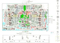
The protection circuit.
Made a snapshot and tied the relevant parts together for clearity.
Notice the minor differences during the production time, in pink along with the serial numbers. Groundings and their routings differ too (another issue...).
From the left & right outputs (before output relay RL901) the dc-levels are sensed through R501/502 and can trip Q501 (-0.6Vdc) or Q502 (+0.6Vdc). Their output is in normal conditions non conductive. Pth 501 keeps a thermal watch. If dc occurs (or pth501 warms up), curent flows towards C147, charging it and tripping Q406. In normal conditions Q406 is off too. During startup, C411 is slowly charged until Q408 switches on, locking along with Q407. If Q406 trips, C411 is discharged, Q408/407 switches off and the relay also.
Check for (dis-) continuities, check the semi's, check the polcaps, check R903 (560Ω/2W) - this one can burn, check D901.
There should be almost no dc on the outputs, also nothing over C501 (should be a bipolar cap actually),
There should be no voltage over C410; C417 (in series with R421 (47k) acts as a 'gate-rail watchdog'.
The voltage over C411 should increase from -44Vdc rail to -43.4Vdc (0.6 above the neg rail).
In the drawing, the outputs are yellow and red (L/R), dc detection is blue, thermal is orange, relay drive is purple (also pre out muting Q206/256 on the filter pcb).
Without the V-fets, the dc on the outputs can be to high and invoke the protection to prevent the relay switching on.
Without the V-fets installed, short C501 temporary to check if the prot-circuit behaves as expected.
Attachments

- Home
- Amplifiers
- Solid State
- Help with Sony TA4650 VFET amp high power supply voltage