Whenever I replace transistors that should be isolated from the heatsinks with silpad or mica I measure with the ohmmeter if all is well.Blitz said:OK, found another faulty insulator
It happens sometimes a faulty one is detected. Saves a lot of trouble afterwards.
Carry one, you'll make it 😉
/Hugo 🙂
So, Checked now all insulators and exchanged quite a lot of them with micas plus CPU-thermal grease from my computer (lessons learned: forget Silpads). Exchanged the 9610 again...and nearly made it: 0,1V Offset (without adjusting anything during warm-up)...
All mosfets showed 0,25V across the source resistor exept of one. This one had 0,4V. Ok, exchanged it. Same result. it was the one which acts as a current source and is connected to the BC550C ( the other 044n on that side is not connected to the BC550C, same principle as in the big Alephs).
OK, Just for testing, detached the BC550C from this mosfet and connected it to the other one: Bingo ! Now the other one showed the 0,4V. OK, exchanged the BC550C again.
Powered it up and start to measure across the source resistor of the current source mosfet which is now connected to the BC550C. Measure nicely, does the expected 0,25V. Slowly then starts to loose Voltage...strange as usually the voltage raises when the amp warms up....OK, let's measure the voltage across the source resistor of the other mosfet (same side, current source, but not connected to the BC550C): ooooooops: 1,2V ! Raising ! So the mosfet must be broken, but how come ?
So, clearly this time all insulators are OK ! Nevertheless I still have the same phenomen as before: When the Rail-Voltage has been raised to 17-18V, The mosfet which is not connected to the BC550C somehow breaks and starts to draw extreme high current.
So, any clues ? Is the BC550C not suitable for this job ? Oszillations ?
Heeeeelp !
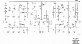
The schematic comes in pieces: As I used hifizen's board, the input piece is Hifizen's with the LM329 option going to the negativ rail and the ZV3306. Instead of MPSA18 I used BC550C. No HF-Caps used across the BC550C. As I get nicely my 3,9V across the 392 source resistor of the 9610, the current source seems to work nicely.
The mosfets are then connected using 0,2mm stranded wire with teflon insulation, star-wired. I know that I could have used thicker cable, but this cable is actually specified up to 6A and as I star-wired everything, it should be no issue, right ? So, there is no mosfet directly conneted to the board, but through p2p-starwire.
The connection from the BC550 is made only to one Mosfet like shown in the schematic.
Attachments
http://www.semiconductors.philips.com/acrobat/datasheets/BC549_550_3.pdf
Unless some connections in your Aleph current source are wrong, I can think of nothing else then the BC550 is wrongly connected.
I assume you use the 100k pot to set the bias. Start with turning that one fully clockwise (or anticlockwise) so it measures 0 Ohm (no voltage across it).
This will limit the bias to an almost harmless current.
Now you should be able to raise the voltage to the target 22V.
If all is well you could slowly start upping the bias with the 100k's.
What bias will you use? Around 5A?
Something I discovered when building mine is that you should properly discharge the supply caps (use something like a big 50 to 100ohm resistor) before you make changes to the circuit. There was always something like +/-5V remaining on them after powering down the amp. This was enough to ruin several mosfets.
/Hugo 🙂
OK, found some errors in wiring where loose connections shortened with others, solved this. Started to fire up again: 9610 are perfectly matched, very same voltages of the source resistor.
After raising to 1,2 A per mosfet same problem again: The mosfet on one side which is not connected to the BC550C draws to much current (3 A), raising...it is always to same one (place) which makes trouble...as the other side simply work wonderful, it is a miracle...well maybe not: I will short the 200k potentiometer next time after having replaced the mosfet again and let's see if this one broke (I turned it already down to 0 Ohm, but you never know I guess)
After raising to 1,2 A per mosfet same problem again: The mosfet on one side which is not connected to the BC550C draws to much current (3 A), raising...it is always to same one (place) which makes trouble...as the other side simply work wonderful, it is a miracle...well maybe not: I will short the 200k potentiometer next time after having replaced the mosfet again and let's see if this one broke (I turned it already down to 0 Ohm, but you never know I guess)
Oh, by the way: I received quite a bit of mails around this threat as many people seem to be eager to understand my errors to avoid them themselfs. So here is another finding: Obviously a variac is essential, otherwise I would have already blown two douzen mosfets more (one dozen though is already killed...)
Heatsinking the rectifier is as well essential...right now they are only mounted on a L-Aluminium-profile and they become hotter than the mosfets themselfs, so I will mount this pieces of metall to the big heatsink before starting any long-term tests.
Heatsinking the rectifier is as well essential...right now they are only mounted on a L-Aluminium-profile and they become hotter than the mosfets themselfs, so I will mount this pieces of metall to the big heatsink before starting any long-term tests.
OK, the poti was dead, I bridged it and now the amp stopped killing mosfets.
Right now I have at 20V:
- 3,701 V across the 9610 left side
- 3,723 V across the 9610 right side
- 0,15 Volt DC at the output
- 13,3 Volt absolute DC measured to ground
- The 200 Ohm Poti at the current source does not do really a difference when playing with it.
So, I guess there are still some issues. I will post some resistor value which I changed as suggested by prominent DIYler of the forum for a high power version of the Aleph-X. MAybe some of these changes are not so wise, so please comment (I refer to Hifizen's schematic above):
- Current source with ZV3306, so R24=392, R26=158, R48=10, R17= 5Mohm, oooops, this one seem to dead as well (was a 0,125W Dale), OPtion J1b
- R14 and R31 = 1k5
- R12 and R34 = 1K
- R1+R4 100Ohm in sum instead of 31 Ohm.
I have as well still variations between mosfets, especially in the current sources (typical 10-20% different). How important is that ? What are your actual values in your amp across the source resistors ?
Overall I have as well one surprise: I have for the actual Amp-Mosfets (so the upper ones) 6A current through them right now at 20 V already. From my calculations this should be the current at 22,7V actually, so how can I get the additional Voltage up without having to exchange the source resistors ?
And: Is 0,15V DC at the output good enough ? How important is the absolute DC-offset of 13 Volt ?
Best REgards
Hi Blitz,
I didn't check this thread in a while, the 13 VDC to gnd at the output is NO GOOD. It means that a group of output mosfets are not properly turned on. From your voltage figures I would guess the gain mosfets are to blame. Don't quote me on that. I don't know what mods you made to the circuit and I don't feel like going thrugh the posts. Simply measure the voltage on the gate output CCS and note the difference between them and the output gain mosftets.
Normally you need to adjust the input CCS to bring it down to by bringing up the voltage from 3.7 to say 4. If the mosfets are selected for equal Vgs and transconductance everything should conduct the same with the same gate voltage.
After the first adjustment let the temp equilibrate and adjust the ccs pot again. If all the output mosfets are matched, adjusting the CCS should produce the same effect on the DC at both outputs. If that doesn't happen you have a matchin problem. In Grey's circuit there were two additional pots available. These provide some room for adjusting the unbalance in the output transistors but you better not rely on them too much.
You are almost there. We'll talk about AC gain adjustment later, you are not quite there,yet. Meanwhile you should have a little talk with the quality control department. 😉
I used silpads in my 50W Aleph X without a problem. Actually I will never use mica again.
just guessing, but if the 200 R pot in the input CCS doesn't make a difference, perhaps it is bad or the value of R26 is too high.
Blitz
What I did in mine was to remove R11 an R33 and the two associated trimpots and substitute them for a 200K trimpot. Now I have a fixed resistor in.
To get more CCS adjustment remove the series parallel around v2 and use a 500ohm trimpot instead. You can initially set all trimpots to half the range. When you are all done you can restrict
the adjustment range of the CCS by removing the pot measuring and making the appropriate series parallel circuit that varies +/- 30 ohms or something.
As usual most of the problems with this circuit can be reconducted back to poor mosfet matching. I am not sure about what % you are talking about but 10 to 20 sounds like too much.
I guess you mean 3.701/3.723 measured from source of 9610 to ground?Blitz said:
Right now I have at 20V:
- 3,701 V across the 9610 left side
- 3,723 V across the 9610 right side
This is not bad, assuming you are talking about DC between +out and –out. The lower you can get it, the better. This is what your speaker finally will see. Be happy with this for the moment.- 0,15 Volt DC at the output
This is way too much and should be less than 1 volt. Lowering VR2 should solve that.- 13,3 Volt absolute DC measured to ground
Measure the voltage at the common source of the 9610’s. When you diminish VR2, the voltage at the sources should go down. Accordingly, the absolute DC should go down too.
I don’t recall exactly but they differ. Not a lot, rather in the mV range. The better matching of mosfets and source resistors, the less variation.I have as well still variations between mosfets, especially in the current sources (typical 10-20% different). How important is that ? What are your actual values in your amp across the source resistors ?
The upper mosfets are the current sources and the lower ones the gain devices.Overall I have as well one surprise: I have for the actual Amp-Mosfets (so the upper ones) 6A current through them right now at 20 V already. From my calculations this should be the current at 22,7V actually, so how can I get the additional Voltage up without having to exchange the source resistors ?
The bias is to be set with the two 100k pots, and should be equal in both the current source resistors and the gain device resistors. From simulations I made this will always be the case with your type of input current source. This is probably due to the J1b options which references to the negative supply (I'm not sure about this so don't pay too much attention to it)). In my AlephX the current source is referenced to ground, similar to the J1a option. This gives a large mismatch in current trough the upper and lower source resistors when absolute DC is not 0.
Carry on, your on the right track 😉
/Hugo 🙂
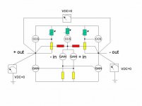
By the way the schematic in post 24 is missing a very important pair of resistors these are in chad's schematic for sure.
Blitz,
Here is a VERY simplified schematic of what I am talking about it completely neglects the AC current gain too but that doesn't matter for the moment. The red resistor is what's missing from the schematic in post 24.
So if all the mosfets are the same, the same voltage drop should be present across the yellow blocks, all the mosfets conduct at the same rate and all the VDC's are 0. That's were you want to be.
Attachments
Ok, replaced the faulty resistor at the current source....
...therefore the 200R pot works now nicely...when setting it to 0 I have only 2,7V absolute DC, but with 7,8V rail voltage I have already 6A through the amp, which is not good. So trimming it higher brings me back to 9,5 V absolute DC on both sides...
Two questions here:
1. I played around with the 200K trimpot. I measured the resistance it gives and had quickly a couple of megaohms ! So it was broken as well. So, what trimpots do you use ? Obviously my 0,5W types are too weak as it has destroyed the on both sides already.
2. On matching: What would be the sequence of matching (in the circuit): First the 9610 and then the mosfets or is everything influencing each other ?
Certainly I have a matching issue: I have with 22V rail voltage (Halleluja ! Nothing smells and I have the right current through the fets now !) the following results:
- V across 392 Resistor of first 9610: 3,8V
- Surprisingly: Now V across the 392 R of the second 9610: 4V. Not good. But does this come from the power mosfets or have the 9610 now changed as they have been matched nicely before (see above) ?
- So Q2 and Q11 are the gain devices, right ? There I have definetly a matching issue as I have between 0,6V and 0,45V across the 0,33R Source resistor.
Lowering VR2 is not really an option as this destroys as well the wanted Rail-Voltage / Current Ratio too much. As stated above VR2 = 0Ohm would give me 2,7V absolute DC-offset ,but 6A already at 7,8V rail voltage...
I changed it to the J1A option. The absolute DC is the same.
Yup, that was an early one and wanted to show only how I connected the mosfets to the BC500C. As I used Hifizen's Board, I used as well the magic two 4k7-resistors (all resistors on the board are 0,1% )
This helps a lot. Thanks you very much for helping me here. One question: In an ideal word all mosfets are perfectly the same. OK. But which pairs should be matched against which pairs best ? With 8 mosfets we have always two pairs:
- gain left side (gl)
- gain right side (gr)
- current source left side (csl)
- current source right side (csr)
So, is it more important for example gl=csl ? Or gl=gr ?
Folks, again thank you very much for your help and encouraging comments. That helps a lot to keep motivation up and work through things. And Grataku, when finished, I will definitely have a serious talk with the guys from my quality control department...
BobEllis said:just guessing, but if the 200 R pot in the input CCS doesn't make a difference, perhaps it is bad or the value of R26 is too high.
...therefore the 200R pot works now nicely...when setting it to 0 I have only 2,7V absolute DC, but with 7,8V rail voltage I have already 6A through the amp, which is not good. So trimming it higher brings me back to 9,5 V absolute DC on both sides...
grataku said:Blitz
What I did in mine was to remove R11 an R33 and the two associated trimpots and substitute them for a 200K trimpot. Now I have a fixed resistor in.
...
As usual most of the problems with this circuit can be reconducted back to poor mosfet matching. I am not sure about what % you are talking about but 10 to 20 sounds like too much.
Two questions here:
1. I played around with the 200K trimpot. I measured the resistance it gives and had quickly a couple of megaohms ! So it was broken as well. So, what trimpots do you use ? Obviously my 0,5W types are too weak as it has destroyed the on both sides already.
2. On matching: What would be the sequence of matching (in the circuit): First the 9610 and then the mosfets or is everything influencing each other ?
Certainly I have a matching issue: I have with 22V rail voltage (Halleluja ! Nothing smells and I have the right current through the fets now !) the following results:
- V across 392 Resistor of first 9610: 3,8V
- Surprisingly: Now V across the 392 R of the second 9610: 4V. Not good. But does this come from the power mosfets or have the 9610 now changed as they have been matched nicely before (see above) ?
- So Q2 and Q11 are the gain devices, right ? There I have definetly a matching issue as I have between 0,6V and 0,45V across the 0,33R Source resistor.
Netlist said:
...
This is way too much and should be less than 1 volt. Lowering VR2 should solve that.
...
This is probably due to the J1b options which references to the negative supply (I'm not sure about this so don't pay too much attention to it)).
/Hugo 🙂
Lowering VR2 is not really an option as this destroys as well the wanted Rail-Voltage / Current Ratio too much. As stated above VR2 = 0Ohm would give me 2,7V absolute DC-offset ,but 6A already at 7,8V rail voltage...
I changed it to the J1A option. The absolute DC is the same.
grataku said:By the way the schematic in post 24 is missing a very important pair of resistors these are in chad's schematic for sure.
Yup, that was an early one and wanted to show only how I connected the mosfets to the BC500C. As I used Hifizen's Board, I used as well the magic two 4k7-resistors (all resistors on the board are 0,1% )
grataku said:Blitz,
Here is a VERY simplified schematic of what I am talking about it completely neglects the AC current gain too but that doesn't matter for the moment. The red resistor is what's missing from the schematic in post 24.
So if all the mosfets are the same, the same voltage drop should be present across the yellow blocks, all the mosfets conduct at the same rate and all the VDC's are 0. That's were you want to be.
This helps a lot. Thanks you very much for helping me here. One question: In an ideal word all mosfets are perfectly the same. OK. But which pairs should be matched against which pairs best ? With 8 mosfets we have always two pairs:
- gain left side (gl)
- gain right side (gr)
- current source left side (csl)
- current source right side (csr)
So, is it more important for example gl=csl ? Or gl=gr ?
Folks, again thank you very much for your help and encouraging comments. That helps a lot to keep motivation up and work through things. And Grataku, when finished, I will definitely have a serious talk with the guys from my quality control department...
"...therefore the 200R pot works now nicely...when setting it to 0 I have only 2,7V absolute DC, but with 7,8V rail voltage I have already 6A through the amp, which is not good. So trimming it higher brings me back to 9,5 V absolute DC on both sides..."
If you are scared of 6A, you shoudn't be because this is a 100W version, use bigger source resistors. You absolutely want be at less than .2V absolute offset and at 20mV between the + and - outputs.
I would match all the gain mosfets in one group and all the CCS mosftets in another. Then match the 9610 the best you can.
The reason is that you can always vary the Vgs on the gain mosftets by increasing the current on the CCS which increases the drop across the 392 ohm resistor. At that point you should always be able to set the output at half the total PS voltage (ie 0 VDC). Basically the difference in voltage drop on the 392's will be equivalent to the DC offset at the speaker.
But you must have two very closely matched 9610. Mismatch is the only reason for the difference across the load resistors.
You definitely have too many broken parts. 😉
Believe it or not I haven't been able to kill a part since I have been playing with Nelsons circuits. I went up to +/- 22V rail with my circuit and .22 ohms source resistors and nothing happened.
The jb2 option has nothing to do with anything. Assuming you wired the board correctly. I was never happy in the way the schematic illustrated the various CCS otpions. Anyways, you may just be biasing the voltage source on the CCS to 20 mA instead of 10 mA but for the moment who cares?
"I was never happy in the way the schematic illustrated the various CCS otpions"
really, it is very confusing. I populated my Aleph-X board and
powered it up and got really whacky readings... i messed up
somewhere... just haven't gotten around to trouble shooting it
yet... shame on me.
really, it is very confusing. I populated my Aleph-X board and
powered it up and got really whacky readings... i messed up
somewhere... just haven't gotten around to trouble shooting it
yet... shame on me.
I smoked 4 fets during the building fase 🙁, the first time was due to wrongly placed bc550C, so the sourceresistors and fets were blown. The second time, 1 fet failed (heatsinks couldn't take the heat).
So you're not the only one 😀. Maybe running 17V and 4,5 A bias has little room for errors with only 4 fets a channel 🙂.
So you're not the only one 😀. Maybe running 17V and 4,5 A bias has little room for errors with only 4 fets a channel 🙂.
Ok, folks, here is the next challenge: As reported I have 9-11V DC. As suggested I measure the voltage over the 392 ohm resistors: 3,8V vs 4 V. OK. Looks like a matching problem, even though I matched them very nicely before. So, I switched sides of the 9610 with each other and: Voila the voltage stays on each side, so the difference does not come from the 9610 ! The 392 resitors are 0,1% types, so that does not give us the difference as well.
The output mosfets are not matched yet really, is there as well a draw back to the 9610 ? I regarded the matching of the mosfets and the matching of the 9610 so far intependantly from each other.
Any ideas what causes the differences in valtage across the two 392 resistors ?
Best Regards
The output mosfets are not matched yet really, is there as well a draw back to the 9610 ? I regarded the matching of the mosfets and the matching of the 9610 so far intependantly from each other.
Any ideas what causes the differences in valtage across the two 392 resistors ?
Best Regards
- Status
- Not open for further replies.
- Home
- Amplifiers
- Pass Labs
- Help needed: Firing up the Aleph-X100