Nope. Each will draw a different current according to their Vgs spec unless matched beforehand. Jfets out of the same bag can vary all over the place.
I agree with Wrench on this one.
Identical Idss precisely measured to ensure identical Vds and identical Pg and identical Tj are exactly selected Idss devices.
Change the Vgs from zero volts to some non zero value and there is no specification for how closely or badly matched the resulting Id.
For Id to remain matched the devices must first be matched for Idss and then matched for Yfs (or gm) such that the same change in Vgs creates the same change in Id.
Glance at the datasheets for confimation of the spread of parameter values for FETs, all FETs. The range in percentage terms is enormous. This is a repeatability problem in manufacture. It has never been overcome. They are getting better but I doubt they will ever get to the small variations that BJT manufacturers seem able to achieve.
Hello,Nope. Each will draw a different current according to their Vgs spec unless matched beforehand. Jfets out of the same bag can vary all over the place.
Thank you guys for your input, I am working towards understanding these JFETS and how to select and use them. Sounds like each one can have a distinct personality.
Speaking of personality, my first trip through the ivory tower I studied Psychology and Statistics. Could be an application for Split-plot ANOVA.
I bet, specified in the cut-sheet or not, there will be some relationships between pairs of parameters. I would be surprised if there is not a clustering of Id values among Idss matched JFETS for example (don’t know).
For grins I think that I will take 50 2SK170-BL’s out of the bag, test and put the results on a spread sheet just to see what shakes out.
The new current meter is scheduled to show up next week.
DT
All just for fun!
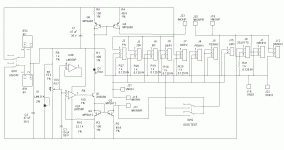
This is a circuit for a "universal" jfet/mosfet matching jig, that also has a socket for LEDs in case you want to check Vf vs If. Two DVMs plug in via tip jacks to measure voltage and current. I came up with this thing to get around the limitations of my first jig, that only has Switchable fixed settings for 1, 2, 5, and 10 ma. Also I found myself needing to match Vf for mosfets, both depletion and enhancement mode, so I needed the extra sockets. It's that, or gin up an adapter, which I always end up losing. The current source is continuously adjustable from ~0 to ~20ma, which is more than enough current for my usual purposes. I included a switch for testing IDSS, but I hardly ever sort for IDSS these days, as Vg vs Id is far more useful. BTW, this is one (just one) application where I feel comfortable using a cheap POS opamp like the LM358.
I just finished building this guy up yesterday, and it works like a charm. Pictures? Maybe...
I just finished building this guy up yesterday, and it works like a charm. Pictures? Maybe...
Attachments
Cool! Yep, it sure looks to cover about everything and a bit more!
OK, now the inevitable questions; some of the acronyms describing the sockets are a bit obscure. Some are obvious but any chance of some detail? Also, what do you suggest for sockets for the through-hole parts and for your DMM connections (2 mm probes, I guess)
U2B, the spare LM358, what purpose to the connection?
Last edited:
The spare 358 is the second opamp in the package, connected up as a follower and left hanging, so it doesn't screw up the opamp in use.
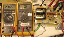
Attached is a picture of the setup, measuring the Vgs of a 2N7000 small-signal mosfet at 10ma Id. I use sockets originally intended for 0.1" spacing headers. These are cheap and allow both TO-92 and TO-220 packages to be readily inserted and removed. When they wear out, I replace them.
Attached is a picture of the setup, measuring the Vgs of a 2N7000 small-signal mosfet at 10ma Id. I use sockets originally intended for 0.1" spacing headers. These are cheap and allow both TO-92 and TO-220 packages to be readily inserted and removed. When they wear out, I replace them.
Attachments
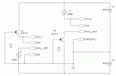
Here is the basic concept behind the sorter, N-Channel and P-Channel flavor. An ammeter is connected between the monitor terminals, and a voltmeter is connected from the source of the device in question to ground. Stopper resistors are connected in series with the DUT gates. I found this eliminated a lot of screwy measurements I was having due to oscillation, especially since there are long DVM leads in the circuit. With a basic setup like this you can then wire up whatever socket pinouts you choose for devices you customarily use, as was shown in the full schematic. I included a "BC" socket (should have been "BF") for Euro-fets. I doubt I'll ever have a chance to use it.
Attachments
Last edited:
Borbely's website seems to be "off the air" -- here's the JFET test jig he described in his 1999 Audio Electronics articles "JFETS" The New Frontier":
You measure Idss by closing the Idss switch. Applying the lower voltage to the source through the 1Meg Ohm resistor gives a good approximation of the pinch-off voltage.
gm is found by calculating dI/dVgs
An externally hosted image should be here but it was not working when we last tested it.
You measure Idss by closing the Idss switch. Applying the lower voltage to the source through the 1Meg Ohm resistor gives a good approximation of the pinch-off voltage.
gm is found by calculating dI/dVgs
An externally hosted image should be here but it was not working when we last tested it.
Hello All,
Looks nice wrenchone.
My tools are getting lonesome, I have been a caregiver lately.
Please share your sorting thoughts. Depending how closely you measure across several variables you could end up with 1000 different groups sorted from a 1000 parts. To get groups large enough of like parts that will work in say a line level crossover or RIAA stage is the goal. What parameter gets measured first then next and so on? The why part is what is interesting. Around the net I see “all you really need to do is…” then there is a short measure of Idss or gm or some other thing.
DT
All just for fun!
Hi,
the two methods of finding gm give different results.
The first gives gm at the current where delta Ids was measured.
At what current does the second equation give a gm value for?
the two methods of finding gm give different results.
The first gives gm at the current where delta Ids was measured.
At what current does the second equation give a gm value for?
At what current does the second equation give a gm value for?
From differentiating Idss with respect to Vgs, this equation:
An externally hosted image should be here but it was not working when we last tested it.
Just a few moments ago, I took a bunch of 2SK170BL which I have binned by Idss of 0.1mA -- from 6 to 11mA. In general the gm within a bin were within a few tenths of a milli-Siemen.
A few years back I looked at a grouping of 100 pcs IRFP240 I received from Avnet -- the transconductance pretty closely matched Vgst.
Hello,
Reflecting back to a time a long time ago dy/dx was the discussed the first day in Calculus 1. For a function, dy is the incremental change in y due to an incremental change in x.
Your statement is that gm is the incremental change in Idss / blah blah blah.
Is Idss not a constant?
DT
All just for fun!
no i understood idss isnt necessarily a constant, idss is measured with reference to a certain operating condition. which is why buying matched jfets that are not matched at same conditions you are going to use is a little misguided. results will still be close, but they will/may not be the same
Last edited:
no i understood idss isnt necessarily a constant, idss is measured with reference to a certain operating condition. which is why buying matched jfets that are not matched at same conditions you are going to use is a little misguided. results will still be close, but they will/may not be the same
Hello,
It was a rhetorical question.
Idss is defined as the drain current with ten volts applied plus the drain and gate grounded.
DT
All just for fun!
If I bother to do a board, it will be with dedicated sockets for most common fet types/pinouts plus common small signal mosfets and no shilly-shallying around. There would be one control to dial in drain current and plug-ins for two monitoring DVMs. This would be similar to what I'm currently using to match fets, but more versatile.
i've found that using a 0.2"/5.08mm pitch screw terminals works great for larger to247, and other larger devices of this ilk and lasts a lot longer than sockets
Hello,
It was a rhetorical question.
Idss is defined as the drain current with ten volts applied plus the drain and gate grounded.
DT
All just for fun!
haha ok sorry, never quite understand posing rhetorical questions on the forus and hadnt read back through the whole thread till now, found yself wondering why you had posed it then refreshed to see this. interesting area thats for sure and one that needs to be explored before any other tweaks in my opinion
TO247 devices are beyond the scope of duties defined for the board I've shown, especially with the board being powered by a pair of 9V batteries. For the larger devices, you also need to worry about heat sinking (surely you won't be trying to characterize an IRFP240 at 10ma) to avoid drift. A dedicated jig with some sort of clamp-on heat sink would be needed.
For those who wondered - the sockets in the jig schematic I posted are pinned out as follows, with pinout read from the flat face/non-mounting surface of the device:
J6 "PN" - for standard NCH TO-92 US devices with pinout DSG
J3 "2SK" - for TO-92 NCH Japanese devices with pinout DGS
J6 "BC" (should be "BF") - for TO-92 Euro devices with pinout GSD
J9 "DEP1" - for NCH depletion mode TO-92 mosfets with pinout SGD
J10 "DEP2" - forNCH depletion mode TO-220 mosfets with pinout GDS
J4 "PENH1" - for PCH enhancement mode mosfets with pinout SGD
J5 "PENH2" - for PCH enhancement mode mosfets with pinout GDS
J15 "LED" - obvious...
All the above are read using the J16 and J17 to monitor current, and J21 and J18 to monitor voltage. VGD/voltage drop will read out as negative.
J8 - "2SJ/J175" - for standard PCH US TO-92 devices and PCH Japanese TO-92 devices with pinout DGS
J1 "NENH1" - for NCH TO-92 enhancement mode mosfets with pinout SDG
J12 "NENH2" - for NCH TO-220 enhancement mode mosfets with pinout GDS
These are read using J23 and J20 to monitor current, and J19 and J22 to monitor voltage. The voltage will read out positive.
It occurs to me that one could also use the enhancement mode sockets for matching Vbe for bipolar devices vs. emitter current. There would be an error due to the base current, but this may be still ok for rough & ready bipolar matching (something I don't do very often, as the bipolars in my designs usually carry spears rather than singing Siegfried...)
IDSS measurement is not optimal for this jig, as the current sense is located in series with the DUT source instead of the drain, so that the meter shunt is providing some degeneration to the DUT. However, the jig as planned provides maximum versatility for measuring VGS vs. Id and forward voltage vs. current for all the devices listed above, which was my main goal. I may never use the IDSS switch. Also, as set up, the enhancement mode devices won't read at all if the switch is set to measure IDSS, keeping one from accidentally zorching devices.
Last edited:
There would be an error due to the base current, but this may be still ok for rough & ready bipolar matching (something I don't do very often, as the bipolars in my designs usually carry spears rather than singing Siegfried...)
Hmm, didn't Siegfried catch a spear in the back in old Niebelheim?
- Status
- Not open for further replies.
- Home
- Source & Line
- Analogue Source
- Help Matching JFET's