I was thinking back on something I read in John Updike's "Bech, A Book" years ago, where the protagonist's mom says to him, "you may not be able to sing Siegfried ( be the lead in opera stuff with brass brassieres and all that), but you can still carry a spear (be an extra)".
The Pass B1 is an excellent example that breaks your rule.
Curl has been telling us for years that jFETs can be biased to 90% of Idss rather than the more usual range of 25% to 75% of Idss.
Curl also reminds us regularly that when Vgs goes slightly +ve, Id exceeds Idss, But, he does warn of excessive gate voltage and it's effect on the gate leakage current.
The Pass B1 and the Salas version referred to as DCB1 are both excellent source followers using jFETs biased at Idss.
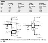
I would like to add this snapshot from Erno Borbelys "Jfets: The New Frontiers, Part 2": Have a look at figure 16B and it´s results in column 4.
Attachments
Hi,
my sims at 20kHz,1V and 5V of the above Buffers resulted in following figures (sims at 1kHz resulted in hardly any better values).
for circuit 16A, idling at an Id of 8.9mA:
THD1V: 0.000024% -132.39dB
K2: 0.000024% -132.9dB
K3: 0.00000141% -157dB
K4: 0.000001024% -160dB
THD5V: 0.000121% -118.3dB
Z(out): 25.6Ohms
for circuit 16B idling at an Id of 14.6mA:
THD: 0.000037% -128.6dB
K2: 0.0000372% -130.5dB
K3: 0.0000014% -157dB
K4: 0.000001057% -160dB
THD5V: 0.000186% -114.6dB
Z(out): 10.3Ohms
K2 dominates, all higher components vanish below the noisefloor.
Even lower figures are reached with a ccs-loaded cascoded JFET.
Like fig. 16A, but omitting with Rd,1M and the 0µ22 cap, replacing the JFETs with a cascode of BF862 (high-gm) and SST4391 (high Vgs) and adding Source resistors of 4.7Ohms to upper and lower leg.
THD: 0.000003% -150.45dB
K2: 0.000002328% -152.7dB
K3: 0.00000122% -158.4dB
K4: 0.00000107% -160dB
THD5V: 0.000009% -140.9dB
Z(out): 33.6Ohms
Here all values remain below the noisefloor, even at 5V output voltage. Noisefloor is at -136dB and slightly higher as with circuits 16A/B. Bandwidth limit is higher. Heat losses in the transistors remain lowest of all 3 circuits. The transfer function is closest to 1.
The introduction of a second source resistor to the upper leg shifts the DC-offset to 0V if the parts are carefully matched, allowing to omit with large DC-coupling caps at the output.
A slight drawback might be that the load impedance to all 3 circuits should be well in the kohms-range if to avoid output voltage drop.
jauu
Calvin
Last edited:
Hi,
I use DVM to take all my measurements. I don't trust ammeters.
A 9V pp3 and a 100r resistor is great for batching jFETs.
use a croc clip or inline socket to short together the G & S.
Apply +ve battery to 100r. Connect 100r to Drain of NjFET
Apply -ve to G+S
A low Idss jFET that draws ~0.5mA will drop ~50mV across the resistor leaving Vds @~8.95V
Pq ~ 0.0005A * 8.95V ~ 4.5mW
Do the same for a medium Idss NjFET. If Idss ~5mA then the Vds ~8.5V and Pq ~45mW ---snip ---
.
I'm feeling really confused right now. Not because of what Andrew wrote, it made perfect sense, and I sorted 100 jfets into batches varying by 1/2 ma IDSS about a year ago.
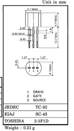
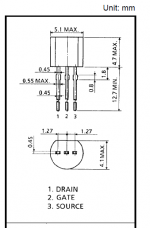
What has me confused is I've just gone to use some of those 2sk170's and looked up the datasheet to check the pinout, and from what I can tell when I tested them (two leads are still together from the testing) I tested with Drain and Gate connected and source connected to power. 😕
I've looked at two copies of the toshiba datasheet tonight. with the jfet flat side up, legs pointing towards me, it shows DGS in one However it looks like when I tested them I thought they were SGD....
Should the test have worked at all if I wired them up the wrong way around? My head hurts....
or is the view the top view?
These are the two different versions of the datasheet picture I found. I suspect the 2nd one is the one I used last time, and to me it looks like it is the view from behind the fet. So which is it??? Is the view in the first pic from the top or the bottom

Tony.
Attachments
I tested with Drain and Gate connected and source connected to power.
Some small signal jfets are symmetrical in terms of D/S.
Hannes
EDIT: found an example, the BF862 jfet from NXP (p.2):
http://www.nxp.com/documents/data_sheet/BF862.pdf
Last edited:
Thanks Hannes, that would explain why they gave me the results I expected. I think I shall do a quick test of a sacraficial jfet 🙂 Those pictures in the datasheet are very hard to interpret, but I would think it would have to be the bottom view.
Tony.
Tony.
Check your Idss with the other legs shorted.
You will find within experimental error that the jFETs measure the same in both directions, provided the gate is always towards -ve (for Nch jFET).
We are lucky with the majority of leg styles that most have the gate in the middle and that reversing the To92 device seems to make little difference.
However, I would not imply from this apparent symmetry that all parameters and performance specifications are identical with D & S swapped.
BTW,
I would not expect any damage to the jFETs by accidentally swapping D & S for the Idss test measurement.
Did you do technical drawing at school?
1st angle projection and 3rd angle projection?
the drawings are both done in 3rd angle projection - look at the object from the position you want your "eye" to be. locate what your eye sees at that viewing point.
Looking from the bottom up at the upper elevation you see the legs pointing towards your eye. locate what you see ( the legs pointing towards your eye) below the elevation.
Similarly looking down at the lower diagram you see the flat face with the curved face mostly hidden from view.
Locate the view as seen from the top at the top.
This layout of the views is quite different from 1st angle. You get used to recognising the different 1st angle and 3rd angle layouts almost instantly. Then the confusion disappears.
The two examples are identical. They both show the elevations (front view) at the top. They both show an "inverted" plan view at the bottom.
Last edited:
Thanks Andrew. I did do tech drawing at school, but only for one year, and it was in 1980 😱 The upper diagram to me looks like from the back, because from the front, all you can see is the front!!! the drawing to me implies looking from the back because it shows two vertical lines which to me would indicate a chamfer (which some transistors have) although these have a radius.
and yes I was a bit worried about whether I might have damaged them!! thanks for the reassurance 🙂
edit: yep just checked one and measures 6.55ma either way around 🙂
Tony.
and yes I was a bit worried about whether I might have damaged them!! thanks for the reassurance 🙂
edit: yep just checked one and measures 6.55ma either way around 🙂
Tony.
I was taught first angle at school, 1964/5
Soon after I left school (while at university) I was shown the difference between 1st and 3rd angle, but continued to draw in 1st.
When I entered industry in 1972, they were just considering moving over to 3rd angle and we always stated on the drawing which we were using.
The schools changed over much later. I did not enter education again until 1996 when schools were teaching 3rd angle.
Remember the rule.
Imagine your eye at the location from which you are viewing. The view as seen by your eye is located at your eye position.
If you are at the top looking down on the lower view then the top view shows what you see from that location. The same applies looking sideways and looking up. What you see from your location is what is located there.
wiki and jeeves were not much help.
http://metal.brightcookie.com/2_draw/draw_t3/htm/draw3_2_5.htm
Last edited:
I think I'll have to sleep on it Andrew (its just past midnight) and my brain just isn't processing it at the moment 🙂
cheers,
Tony.
cheers,
Tony.
Well, third angle is pretty clear but in 1964/5 when had to accommodate both projections of drafting , I did get confused..... but I would think it would have to be the bottom view. Tony.
Whether the drawing has been correctly laid out or not, the pin assignments can't be reversed in adjacent projections - they must align vertically or horizontally in adjacent views. I'd try to simplify the explanation (I hope).
In 3rd angle, the closest face of an adjacent view should be what you see in your current view.
In 1st angle you see the opposite one.
That's about all the projection symbol tells you.
Last edited:
thanks guys, I see what you were saying now, the pin positions in the top and bottom drawings have to be the same. they cannot be transposed, so the bottom view is obvious as viewing from the top there would be no pins, so it is not ambiguous.
It does make me think it is a strange drawing of the front of the transistor though. unless the case curves in slightly (ie front face is not the widest part of the jfet body) and I just didn't notice.
Tony.
It does make me think it is a strange drawing of the front of the transistor though. unless the case curves in slightly (ie front face is not the widest part of the jfet body) and I just didn't notice.
Tony.
- Status
- Not open for further replies.
- Home
- Source & Line
- Analogue Source
- Help Matching JFET's