Hi Edmond,
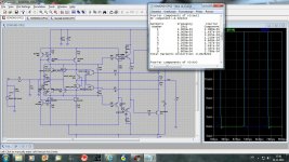
Here is what I get simulating with LTspice. I used mostly the same transistor(THAT also) and my result are quite different.
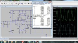
Total Harmonic Distortion: 0.176320% at 20kHz.
Attached simulation where FFT and output BJTs currents can be seen.
Damir
Hi Damir
It's impossible to see your schematic, you have to post something that is readable.
I guess you understand that you have to adjust some values (to make the circuit work optimally) when you use different devices.
The THD will be low in Edmond's OPS but will it be stable?
BTW: Edmond is in Paris this week.
Cheers
Stein
Hi Stinius,
I did an error on the firts schematic, Q7 was up side down. Here is correct schematic and simulation results with 30V and 2V at the input. It is interesting that the distortion doubled at lower level.
Damir
Attachments
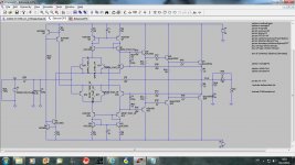

The input LTPs appear to have both the emitters commoned and the collectors commoned.
That's correct - it is a Class I output stage. It featured in Jan's Linear Audio (vol 2).
That's correct - it is a Class I output stage. It featured in Jan's Linear Audio (vol 2).
Yep,
I really enjoyed that article, really a very clever approach.
Highly recommended.
Hope this helps
-Antonio
Hi Edmond,
[snip]
I think that this could work with your OPS or Kendall. What is your opinion?
Damir
Hi Damir,
After some thoughts and some simulations, I have changed my mind. It appears that without emitter followers in front of my version, the input impedance is still pretty high: in the order of one MOhms. This means that the circuit can be simplified, as you don't need provisions for biasing the EF stages any longer. In fact, it's even simpler than Kendall's version. Moreover, the input impedance doesn't varies so widely and the NFB loop response doesn't varies with output current.
The distortion is of the same order: around 50ppm @ 20kHz.
The only con is a slightly higher tempco of the OPS quiescent current: 0.3%/K versus 0.1%/K of Kendall's circuit (not a real; problem I would think)
> Regarding thermal stability, what transistors should be thermaly connected(to the output transistors or maybe not)?
The THAT300, respectively THAT320 trannies should be thermally coupled to each other (that's why I've chosen these IC's). Furthermore, Q3 to Q9, respectively Q6 to Q12.
No thermal coupling to the output trannies. That's the virtue of auto-bias.
There's one thing both circuit's don't like: square waves, as it will lead to severe cross-conduction of the output devices (with fatal results).
Also, be careful with triple EF output stages, as it's said that they are prone to oscillations. Regrettably, I have no experience with them. Perhaps other members can advise you on that.
Below a basic example of the alternative version. I've forgot to add a Zobel network, which you really need for stability.
Cheers,
E.
Attachments
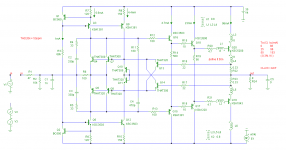
Oops, there's a small error in the schematic: Q10 & Q11 have wrong type numbers.
See below for a correction.
edit: Not only the Zobel network is missing, also some clamp/protection diodes are not shown.
See below for a correction.
edit: Not only the Zobel network is missing, also some clamp/protection diodes are not shown.
Attachments
Last edited:
Class-I
I observed that too! One more reason to go for my version. 😀
Hi Stinius,
.................
It is interesting that the distortion doubled at lower level.
Damir
I observed that too! One more reason to go for my version. 😀
AutoBias-II
For those who aren't happy with the tempco of Iq, here's a version with a near zero tempco (that is, under the premise that Q1, Q2 and the THATs are held at the same (ambient) temperature).
edit: This accomplished by inserting R8, R9, R11, R12 and adjusting the CCSes to equal currents.
Please, notice that a short circuit protection is still missing.
Regarding nasty test signals (e.g. square waves), don't torture this amp with transients slewing more than 100V/us.
Cheers,
E.
Attachments
Last edited:
Hi Edmond,
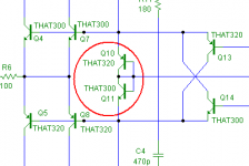
Why there two transistors in parallel, Q4//Q7 and Q5//Q8? This is not Class i driver?
Damir
Why there two transistors in parallel, Q4//Q7 and Q5//Q8? This is not Class i driver?
Damir
Hi Edmond,
Why there two transistors in parallel, Q4//Q7 and Q5//Q8? This is not Class i driver?
Damir
Hi Damir,
Good question. You can make it work with only one pair of them, but then you have to halve the output current of Q3 and Q6. As the current ratio between first pair of CCSes (Q3/Q6) and the second par (Q9/Q12) is rather critical, I prefer a 1:1 ratio (instead of 1:2), which is easier to maintain. In that case however, you will need Q7/Q8 as well. Overkill? Not at all! It cost you nothing as there are already four trannies per IC.
>This is not Class i driver?
That's right. And let's keep it that way. 😉
I'm through with Class-I, as it is suboptimal.

Cheers,
E.
I'm through with Class-I, as it is suboptimal.
Cheers,
E.
I Agree 🙂
BTW: The harddisk has crashed on my main PC, hopefully I'm able to restore it, otherwise alot of things are gone. 😡
Hope you had a nice week in Paris.
Cheers
Stein
Hi Edmond,
Referring to post 429, what is the function of D1 & D2?
Are D1 & D2 needed in the schematic of post 426 - http://www.diyaudio.com/forums/soli...ogy-construction-troubles-43.html#post2816967
Thanks,
Ian
Referring to post 429, what is the function of D1 & D2?
Are D1 & D2 needed in the schematic of post 426 - http://www.diyaudio.com/forums/soli...ogy-construction-troubles-43.html#post2816967
Thanks,
Ian
Hi Damir,
Good question. You can make it work with only one pair of them, but then you have to halve the output current of Q3 and Q6. As the current ratio between first pair of CCSes (Q3/Q6) and the second par (Q9/Q12) is rather critical, I prefer a 1:1 ratio (instead of 1:2), which is easier to maintain. In that case however, you will need Q7/Q8 as well. Overkill? Not at all! It cost you nothing as there are already four trannies per IC.
>This is not Class i driver?
That's right. And let's keep it that way. 😉
I'm through with Class-I, as it is suboptimal.
Cheers,
E.
Hi Edmond,
What is output impedance?
Damir
I Agree 🙂
Hi Stein,
At first sight, class-I looked very promising. However, there are too many quirks: a rather low and highly variable input impedance as well as a variable loop response. As for the latter, you can't optimize it for all dynamic conditions (i.e. low and high output currents). As a result, you need almost as much as two times more frequency compensation in order to cope with the worst case condition.
The only pro is more headroom (1 Vbe) for the bias/class-i circuitry.
BTW: The hard disk has crashed on my main PC, hopefully I'm able to restore it, otherwise a lot of things are gone. 😡
Too bad.
 Can you tie the HD on another PC? Much change to recover most of your data.
Hope you had a nice week in Paris.
Cheers
Stein
Sure, we had a nice time; thanks.
BTW, do you have copies of syn08 posts on the 'other' forum about triple EF output stages? It's a pity that Andy has closed that site.
Cheers,
E.
Hi Edmond,
Referring to post 429, what is the function of D1 & D2?
Hi Ian,
D1 & D2 prevent saturation and excessive base currents of Q4/5/7/8 under overload conditions (e.g. square waves).
Are D1 & D2 needed in the schematic of post 426 - http://www.diyaudio.com/forums/soli...ogy-construction-troubles-43.html#post2816967
Thanks,
Ian
Yes, indeed. They are also needed in this version (unless you can guarantee that you will never torture the amp 😉 )
Cheers,
E.
Output impedance
Hi Damir,
About 0.7 mOhm (real) and it starts rising at ~3kHz, where it becomes inductive. At 10kHz Zo = 1.7 mOhm and at 100kHz Zo = 16 mOhm (without Zobel network, of course).
As you see, much lower than Kendall's class-i, where Zo = RE = 330 mOhm.
Cheers,
E.
Hi Edmond,
What is output impedance?
Damir
Hi Damir,
About 0.7 mOhm (real) and it starts rising at ~3kHz, where it becomes inductive. At 10kHz Zo = 1.7 mOhm and at 100kHz Zo = 16 mOhm (without Zobel network, of course).
As you see, much lower than Kendall's class-i, where Zo = RE = 330 mOhm.
Cheers,
E.
Last edited:
Hi Damir,
About 0.7 mOhm (real) and it starts rising at ~3kHz, where it becomes inductive. At 10kHz Zo = 1.7 mOhm and at 100kHz Zo = 16 mOhm (without Zobel network, of course).
As you see, much lower than Kendall's class-i.
Cheers,
E.
Hi Edmond,
I expected that, Class i gives it equal to Re.
Damir
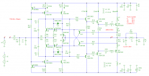
Hi Edmond,
Here is my simulation of yours OPS.
Distortion is realy low, but the current of inactive output transistor dip below zero.
Could you explain? Does your OPS is non switching type? Could you show some charts of your simulatio, main could be wrong.
Damir
Here is my simulation of yours OPS.
Distortion is realy low, but the current of inactive output transistor dip below zero.
Could you explain? Does your OPS is non switching type? Could you show some charts of your simulatio, main could be wrong.
Damir
Attachments
- Home
- Amplifiers
- Solid State
- HEEEELLLPPP : M. Randy Slone Mirror Image Topology Construction - Troubles