Hi Olivier,
The decoupling caps C24 and C25 are too low, and for the Miller test increase C7 to 1kF.
I've asked you this before: please use my files; it take hours to debug your files.
Cheers,
E.
The decoupling caps C24 and C25 are too low, and for the Miller test increase C7 to 1kF.
I've asked you this before: please use my files; it take hours to debug your files.
Cheers,
E.
does.........for the Miller test increase C7 to 1kF.
1kF = 1000F ?
Hi Edmond,
I didn't notice the feedback capacitor was a little bit sized up from 470u tu 1k. I only noticed the shorted feedback resistor. On the schematic it is less visible than it would be in reality. About the decoupling caps I didn't check them as I had no idea this could impact the AC analyses somehow. The final result is the same anyway 50MHz ULGF with around 66° of PM.
This is not the best of figures maybe but it's because the millercaps are 22p now (i placed them to push te amp a bit)
So now I know how to simulate the millerloop and cmcl loop !!! Thanks !!!
The OPS you showed in one of your last posts seems to have impressive results and got my attention.
If you agree we could optimize it and make a pcb for it?
Yes, I will use your files ... I suppose I start with schematic RS10-Vert? Or have you changed something since? However the RS10 file does not contain the OPS4 outputstage which seems to be the choice?
Cheers,
Olivier
Hi Edmond,
I didn't notice the feedback capacitor was a little bit sized up from 470u tu 1k. I only noticed the shorted feedback resistor. On the schematic it is less visible than it would be in reality. About the decoupling caps I didn't check them as I had no idea this could impact the AC analyses somehow. The final result is the same anyway 50MHz ULGF with around 66° of PM.
This is not the best of figures maybe but it's because the millercaps are 22p now (i placed them to push te amp a bit)
Hi Olivier,
Indeed, the Miller caps are too small, but remember, he final value (also of the other compensation stuff) depends on the load of the OPS, which isn't defined yet.
So now I know how to simulate the millerloop and cmcl loop !!! Thanks !!!
You're welcome.
The OPS you showed in one of your last posts seems to have impressive results and got my attention.
If you agree we could optimize it and make a pcb for it?
NOOOOOOOOOOOOOOOOOO, not that fast.
1. You had a lot of other questions, that have to be answered first.
2. OPS4 has issues. Do NOT build this one.
The trouble is that I've discovered some instability (due to a pos. FB loop) and I don't know yet how to tackle it. Whether it's solvable at all, I don't know either as I haven't seen the original paper from Kendall yet.
To all: Has nobody read Kendall's article and/or is willing to send me a copy?
Yes, I will use your files ... I suppose I start with schematic RS10-Vert? Or have you changed something since? However the RS10 file does not contain the OPS4 output stage which seems to be the choice?
Cheers,
Olivier
>does not contain the OPS4 output stage
See above.
Cheers,
E.
Good evening Edmond,
I have noticed some other changes in the schematic. Could you tell me why the change is made?
1) the diodes in the diff amp, right legs, are replaced by zener diodes D3/4 value 4V7?
With simple diodes the clamp doesn't work correctly. The voltage drop across the diodes should be equal to the v-drop across D11 respectively D12 (and in turn D19 resp. D20).
2) The resistors in the current source legs are replaced by zeners D5/6 value 4V7 (you already mentioned this change)?
I've replace the 1K resistors by these Zener to improve the temp. stability. The voltage drop across the original resistors serves as a reference for CMCL. However, the current CCSes have a distinct tempco. As a result, the CMCL will also alter with temperature and I didn't like it. Hence the Zeners to improve it somewhat. When stable CCSes are installed, you can put the resistors back.
3) The feedback capacitor had a parallel leg which included a polypropylene capacitor. Is it useless or just deleted for simulation purpose?
Just deleted for simulation purpose (I was just lazy).
4) The sequence of connection to the rails of the decoupling capacitor is particular. Is that how it should be intended on the PCB too? First it is placed between the VAS and IPS. Second, the RC filter between VAS and IPS is right in between both decoupling capacitors (the electrolyt C12 and the non polarized smaller one C8).
The position of these caps is unrelated to the position on the PCB. I put theme there, just because there was some room.
5) The non polarized caps are 10 fold larger. Is this really better?
Do you mean C5? I increased the value only for simulating purposes.
6) C6 and C7 are of different value? I suppose it's a copy paste error.
I forgot to alter C7 to 47u
7) Q21 and Q22 are 2N5551 & 2N5401 Q's whereas it was 2SC3503 and 2SA1381. In my circuit the developed power is very limit. In yours the power is lower. Why lower? Better lower?
I thought, erroneously!, you were using 2N5551 & 2N5401. Taking the power dissipation into account, 2SC3503 and 2SA1381 are more suitable.
8) Zeners D11 & D12 are changed from 6V2 to 4V7 equal to the cascode zeners. I made them slightly higher in order to be sure the cascodes cannot saturate. Is that wrong thinking then?
No, that is not 'wrong thinking', but a minimum Vce of 0.7V is safe. Any increase of this voltage goes at the expense of of the max output swing, which is already reduced by the use of cascodes.
9) C17 A & B are removed. Are they useless?
Probably yes, though I'm not 100% sure (depends on future modifications and/or new issues which are not discovered yet). If it's not a problem, just reserve some room and holes on the PCB for these components.
I suppose we could replace all or most zeners by voltage references?
Yes, 2.5V for example (plus a diode).
As for the OPS devices lets keep them Laterals 1058/162. The only bummer is the voltage limit 160V :-(
I will also look for higher voltage devices.
By the way what do you think of IRFP9240? Is vertical mosfet.
>IRFP9240?
A horrible device.
Try to find 2SJ201 (and 2SK1530)
If you opt for an 'autobias' circuit, vertical MOSFETs, which have a higher Vgth, make things much easier. This is because an autobias circuit needs some headroom and a Vgth of near zero volt provides no headroom at all (I know, this might be solved too, that is, by mean of a kludge. Not my cup of thee)
Cheers,
E.
Good evening Edmond,
OK about the OPS let's go for the RS10 version. OPS4 is a parallel developpement you are doing if I'm right. I suppose you mean, getting OPS4 working will push the project I am willing to implement too far in the future. Unless there is a breakthrough in OPS4 before RS10 is transferred completely to PCB.
I understand all your replies to my previous questions. I agree.
Well, do you think it would be a good thing to lower the millercaps until reaching the point where the IPS/VAS/dummyOPS starts to oscillate? Probably not (anyway I don't have ceramics under 22p, lower caps are PP type and are more expensive + very short leads to place it flying over the board). The reason is I would like to know if the PCB is designed well or not. E.g for parasitic caps etc.
What are according to you weak points about the RS10 if any? What should be worked on?
No problem to switch to verticals. The devices you name are discontinued it seems and will thus be hard to get. But we'll see.
I post back (surely) if I have questions about RS10 (ops part).
Cheers,
Olivier
Edmond,
About the first leg in the VAS stage I opted for 2SA/SC devices to be able to raise the current in that leg. That's because I noticed zeners need quite some current to be well in their zener region.
I will change them to the larger devices in the RS10 file and rename it RS10.01.
Cheers
Olivier
About the first leg in the VAS stage I opted for 2SA/SC devices to be able to raise the current in that leg. That's because I noticed zeners need quite some current to be well in their zener region.
I will change them to the larger devices in the RS10 file and rename it RS10.01.
Cheers
Olivier
Good evening Edmond,
OK about the OPS let's go for the RS10 version. OPS4 is a parallel developpement you are doing if I'm right. I suppose you mean, getting OPS4 working will push the project I am willing to implement too far in the future. Unless there is a breakthrough in OPS4 before RS10 is transferred completely to PCB.
Hi Olivier,
You're right, getting OPS4 working will push the project too far in the future. The more so as Kendall's circuit does have some issues: it's not in every respect perfect. The alternative, my atobias version II, is less prone to oscillations, but it's even more complicated. Besides, it has never been built yet. So it's not the most obvious circuit to start with (and asking for troubles).
I understand all your replies to my previous questions. I agree.
Well, do you think it would be a good thing to lower the millercaps until reaching the point where the IPS/VAS/dummyOPS starts to oscillate?
Hmm.... a dangerous approach, because in real life, with reactive speaker loads etc, you might need more phase margin.
probably not (anyway I don't have ceramics under 22p, lower caps are PP type and are more expensive + very short leads to place it flying over the board). The reason is I would like to know if the PCB is designed well or not. E.g for parasitic caps etc.
What are according to you weak points about the RS10 if any? What should be worked on?
RS10 is a good starting point, though I have to work it out and see if there are any issues which I've overlooked and/or not yet discovered. So please wait with the PCB artwork.
No problem to switch to verticals. The devices you name are discontinued it seems and will thus be hard to get. But we'll see.
I post back (surely) if I have questions about RS10 (ops part).
Cheers,
Olivier
Cheers,
E.
Class-I
Hi Damir,
You may compare the distortion of the Kendall/Nakayama OPS with my version. However, for frequencies in the upper audio spectrum multiply these figures by two. This is because his OPS needs twice as much frequency compensation to get the same level of stability.
Furthermore, it should be noticed that the input impedance of Kendall's OPS is rather low, around 50kOhms and, according him, also highly nonlinear. So it's not recommended to tie this OPS directly to a VAS output. Instead, put a buffer in between.
Other versions of AB2-EC-V4 output stage can be found here and a patent on the class-I OPS can be found there.
As an aside, the funny things is that I already simmed the Kendall/Nakayama OPS a couple of years ago, although didn't pay much attention to it (probably I wasn't impressed) and forgot the hole thing until Jan Didden shows up with Kendall's article in his 'bookzine' (just another coincidence? 🙄).
Cheers,
E.
Very interesting. Can you give some simulation numbers? It's a pity I can not use your file for LTspice.
dado
Hi Damir,
You may compare the distortion of the Kendall/Nakayama OPS with my version. However, for frequencies in the upper audio spectrum multiply these figures by two. This is because his OPS needs twice as much frequency compensation to get the same level of stability.
Furthermore, it should be noticed that the input impedance of Kendall's OPS is rather low, around 50kOhms and, according him, also highly nonlinear. So it's not recommended to tie this OPS directly to a VAS output. Instead, put a buffer in between.
Other versions of AB2-EC-V4 output stage can be found here and a patent on the class-I OPS can be found there.
As an aside, the funny things is that I already simmed the Kendall/Nakayama OPS a couple of years ago, although didn't pay much attention to it (probably I wasn't impressed) and forgot the hole thing until Jan Didden shows up with Kendall's article in his 'bookzine' (just another coincidence? 🙄).
Cheers,
E.
Hi Edmond,
You said in your previous post that you have seen very basic sketch of Kendall/Nakayama OPS and made what you think is close to original circuit. I would like to compare those two OPSs, but to do it in LTspice from your schematic I am not sure how to implement drivers before output transistors. How much room the Autobias and Error Feedback circuit needs for Kendall/Nakayama OPS? I prefere to use BJT for output transistors as I have some spares. I would need that kind of OPS to be directly driven by my Aikido tube preamp.
Could you suggest practical schematic?
Damir
Class I
Hi Edmond
I'm back home and had a glance on the Class I ops, I'm dissapointed, the circuit has serious oscillation problems.
When I mentioned the Class I ops in the "Linear Audio" thread I hoped it would be a lot better design, but no.
BTW: I don't have the original Class I article, so if somebody could scan it and email to me I would appreciate it. 🙂
@ Dadod, I think you can put the circuit into LTspice without any problems, if you want the ops driven directly by a preamp it will not be loud, you will need a so called VAS (TIS) in between.
Cheers
Stein
Hi Edmond,
You said in your previous post that you have seen very basic sketch of Kendall/Nakayama OPS and made what you think is close to original circuit. I would like to compare those two OPSs, but to do it in LTspice from your schematic I am not sure how to implement drivers before output transistors. How much room the Autobias and Error Feedback circuit needs for Kendall/Nakayama OPS? I prefere to use BJT for output transistors as I have some spares. I would need that kind of OPS to be directly driven by my Aikido tube preamp.
Could you suggest practical schematic?
Damir
Hi Damir,
In both cases I foresee issues:
Although the autobias-II circuit is suitable to be driven by tubes (as it has a very high input impedance) it has too less headroom to drive BJTs.
Regarding Kendall's circuit, the driver section of this one has more headroom (1xVbe), but the input impedance is rather low and nonlinear. If you drive this circuit by tubes, you will need additional emitter followers (which add to complexity) in order to keep the distortion within acceptable levels.
BTW, YGM.
Cheers, E.
Claas-I
Hi Stein,
The oscillation problems are not that serious. You simply need more compensation, i.e. lower the ULGF of the NFB loop. I also observed that the loop properties depend on the amount of current delivered to the output load. I feel uncomfortable with this 'feature'.
Cheers,
E.
(later this evening YGM)
Hi Edmond
I'm back home and had a glance on the Class I ops, I'm dissapointed, the circuit has serious oscillation problems.
When I mentioned the Class I ops in the "Linear Audio" thread I hoped it would be a lot better design, but no.
BTW: I don't have the original Class I article, so if somebody could scan it and email to me I would appreciate it. 🙂
@ Dadod, I think you can put the circuit into LTspice without any problems, if you want the ops driven directly by a preamp it will not be loud, you will need a so called VAS (TIS) in between.
Cheers
Stein
Hi Stein,
The oscillation problems are not that serious. You simply need more compensation, i.e. lower the ULGF of the NFB loop. I also observed that the loop properties depend on the amount of current delivered to the output load. I feel uncomfortable with this 'feature'.
Cheers,
E.
(later this evening YGM)
>Although the autobias-II circuit is suitable to be driven by tubes (as it has a very high input impedance) it has too less headroom to drive BJTs.
Hi Damir,
Above sentence is probably too cryptic and ill formulated.
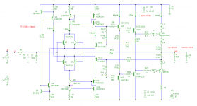
I mean when my auto bias circuit is connected to a BJT OPS and when also using separate push-pull driver stages ( shown here: here, Q7...Q10), then the headroom (Vce) of the bias circuit becomes too low.
However, in case of a conventional triplet (instead of separate PP drivers), then there is still enough headroom: 1.9V. See below for a possible implementation.
BUT... there's another problem. Where to get the bias voltages (V4 and V5)? Normally, you can 'steel' these voltages from the VAS. However, when operated in isolation, e.g. when tied your tube pre-amp, there is nothing to 'steel' and you need extra circuitry to bias the input stage (Q1 & Q3).
BTW, THD20 is one quarter of Kendall's circuit.
In order to keep things more simple, let's go back to Kendall's OPS, as this one hasn't input bias issues. OTOH, it has input impedance issues. At quiescent conditions Zi is about RL * beta^2 (80kOms or so), but varies considerably with output current: If Io = 1A -> Zi > 10MOhms.
Now all depends on the the output impedance of your tube pre-amp. If sufficiently low (in case of a cathode follower) you might use Kendall's OPS, but has it sufficient gain and output swing? Only you can answer these questions.
Cheers,
E.
PS: Whenever possible, I prefer separate PP drivers, which help to prevent cross-conduction of the output devices, as the ubiquitous speedup cap (see C7) is an absolute no no. BTW, this applies to all output stages with a (fast acting) variable bias. C7 should kill the whole concept.
edit: One more thing: my circuit suffers from some offset voltages (depending on mismatch between Q1 and Q3)
Hi Damir,
Above sentence is probably too cryptic and ill formulated.
I mean when my auto bias circuit is connected to a BJT OPS and when also using separate push-pull driver stages ( shown here: here, Q7...Q10), then the headroom (Vce) of the bias circuit becomes too low.
However, in case of a conventional triplet (instead of separate PP drivers), then there is still enough headroom: 1.9V. See below for a possible implementation.
BUT... there's another problem. Where to get the bias voltages (V4 and V5)? Normally, you can 'steel' these voltages from the VAS. However, when operated in isolation, e.g. when tied your tube pre-amp, there is nothing to 'steel' and you need extra circuitry to bias the input stage (Q1 & Q3).
BTW, THD20 is one quarter of Kendall's circuit.
In order to keep things more simple, let's go back to Kendall's OPS, as this one hasn't input bias issues. OTOH, it has input impedance issues. At quiescent conditions Zi is about RL * beta^2 (80kOms or so), but varies considerably with output current: If Io = 1A -> Zi > 10MOhms.
Now all depends on the the output impedance of your tube pre-amp. If sufficiently low (in case of a cathode follower) you might use Kendall's OPS, but has it sufficient gain and output swing? Only you can answer these questions.
Cheers,
E.
PS: Whenever possible, I prefer separate PP drivers, which help to prevent cross-conduction of the output devices, as the ubiquitous speedup cap (see C7) is an absolute no no. BTW, this applies to all output stages with a (fast acting) variable bias. C7 should kill the whole concept.
edit: One more thing: my circuit suffers from some offset voltages (depending on mismatch between Q1 and Q3)
Attachments
Last edited:
>Although the autobias-II circuit is suitable to be driven by tubes (as it has a very high input impedance) it has too less headroom to drive BJTs.
Hi Damir,
Above sentence is probably too cryptic and ill formulated.
I mean when my auto bias circuit is connected to a BJT OPS and when also using separate push-pull driver stages ( shown here: here, Q7...Q10), then the headroom (Vce) of the bias circuit becomes too low.
However, in case of a conventional triplet (instead of separate PP drivers), then there is still enough headroom: 1.9V. See below for a possible implementation.
BUT... there's another problem. Where to get the bias voltages (V4 and V5)? Normally, you can 'steel' these voltages from the VAS. However, when operated in isolation, e.g. when tied your tube pre-amp, there is nothing to 'steel' and you need extra circuitry to bias the input stage (Q1 & Q3).
BTW, THD20 is one quarter of Kendall's circuit.
In order to keep things more simple, let's go back to Kendall's OPS, as this one hasn't input bias issues. OTOH, it has input impedance issues. At quiescent conditions Zi is about RL * beta^2 (80kOms or so), but varies considerably with output current: If Io = 1A -> Zi > 10MOhms.
Now all depends on the the output impedance of your tube pre-amp. If sufficiently low (in case of a cathode follower) you might use Kendall's OPS, but has it sufficient gain and output swing? Only you can answer these questions.
Cheers,
E.
PS: Whenever possible, I prefer separate PP drivers, which help to prevent cross-conduction of the output devices, as the ubiquitous speedup cap (see C7) is an absolute no no. BTW, this applies to all output stages with a (fast acting) variable bias. C7 should kill the whole concept.
edit: One more thing: my circuit suffers from some offset voltages (depending on mismatch between Q1 and Q3)
Hi Edmond,
Thank a loot for your help.
I intend to use Aikido(http://www.tubecad.com/Product_PDFs/9-Pin_Stereo_Rev_C.pdf) integreted with the OPS in the same box. Aikido is posible to configurate to have enough gain(12AX7) and quite low output impedance(output tube configurated as White cathode-follower). The gain could be set to a bit more the 40 and output impedance could be a bit more then 50ohm with 6H30 tube. I think that this could work with your OPS or Kendall. What is your opinion?
Damir
Class-I
Hi Damir,
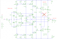
In this special case I would go for Kendall's OPS, that is, after some modifications: matches trannies (THAT300/320) for the bias circuitry and provisions for equal Vce (around 2.7V) of the THATs by means of Q8,9,14,15. Below a proposal. Not shown: decoupling caps and the Zobel network.
I'm not 100% sure about the base stoppers and frequency compensation. Perhaps other values are needed.
Cheers,
E.
edit: I forgot two caps of 100nF. One between the base of Q13 and the pos. supply rail; the other between the base of Q18 and the neg. supply rail.
Hi Damir,
In this special case I would go for Kendall's OPS, that is, after some modifications: matches trannies (THAT300/320) for the bias circuitry and provisions for equal Vce (around 2.7V) of the THATs by means of Q8,9,14,15. Below a proposal. Not shown: decoupling caps and the Zobel network.
I'm not 100% sure about the base stoppers and frequency compensation. Perhaps other values are needed.
Cheers,
E.
edit: I forgot two caps of 100nF. One between the base of Q13 and the pos. supply rail; the other between the base of Q18 and the neg. supply rail.
Attachments
Last edited:
Hi Damir,
In this special case I would go for Kendall's OPS, that is, after some modifications: matches trannies (THAT300/320) for the bias circuitry and provisions for equal Vce (around 2.7V) of the THATs by means of Q8,9,14,15. Below a proposal. Not shown: decoupling caps and the Zobel network.
I'm not 100% sure about the base stoppers and frequency compensation. Perhaps other values are needed.
Cheers,
E.
edit: I forgot two caps of 100nF. One between the base of Q13 and the pos. supply rail; the other between the base of Q18 and the neg. supply rail.
Hi Edmond,
Regarding thermal stability, what transistors should be thermaly connected(to the output transistors or maybe not)?
Damir
Hi Damir,
In this special case I would go for Kendall's OPS, that is, after some modifications: matches trannies (THAT300/320) for the bias circuitry and provisions for equal Vce (around 2.7V) of the THATs by means of Q8,9,14,15. Below a proposal. Not shown: decoupling caps and the Zobel network.
I'm not 100% sure about the base stoppers and frequency compensation. Perhaps other values are needed.
Cheers,
E.
edit: I forgot two caps of 100nF. One between the base of Q13 and the pos. supply rail; the other between the base of Q18 and the neg. supply rail.
Hi Edmond,
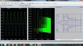
Here is what I get simulating with LTspice. I used mostly the same transistor(THAT also) and my result are quite different.
Total Harmonic Distortion: 0.176320% at 20kHz.
Attached simulation where FFT and output BJTs currents can be seen.
Damir
Attachments
- Home
- Amplifiers
- Solid State
- HEEEELLLPPP : M. Randy Slone Mirror Image Topology Construction - Troubles