After long hesitate and couple of PMs, I decided to open this thread.
Inspired by diyaudio member Dadod's thread, I've built power amplifier with Hawksford error correction scheme (HEC).
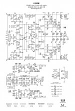
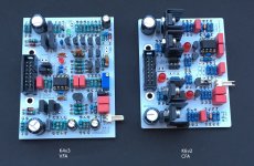
It's a split design, IPS and OPS. They are not enclosed by global feedback loop (which is not totally true, IPS has a jumper to set it, but only for testing purpose). There are two versions of OPS (diamond buffer quadruple), bipolar (3 pairs of NJW0281/0302) and hexfet (3 pairs of IRFP240/9240). It can deliver 200/170 Watt into 4 ohms, pcb is common for both types. Measured thd1 was 0.003% 50W@4.5ohm (or better, sound card limitation), slew-rate 120V/us.
K200 - OPS bjt, stable, built (schematic v1.5, pcb v2.2)
https://picasaweb.google.com/106882583920049206569/K20002?authuser=0&feat=directlink
K200M - OPS hexfet, under development (schematic v1.1, pcb v2.2)
https://picasaweb.google.com/106882583920049206569/K200M?authuser=0&feat=directlink
K4 - IPS vfa (blameless), stable, built (schematic v2.3, pcb v2.0)
https://picasaweb.google.com/106882583920049206569/K4Frontend?authuser=0&feat=directlink
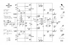
K5 - IPS cfa, stable, built (schematic v1.2, pcb v1.0)
https://picasaweb.google.com/106882583920049206569/K5Frontend?authuser=0&feat=directlink
ProtectOne - auxiliary circuits, built (schematic v1.0, pcb v1.0)
* on/off toggle switch
* transformer soft-start
* mains LC filter
* loadspeaker protection (DC, delay)
* OPS RL network
https://www.youtube.com/watch?v=QMYUAJ7LMV4

I am rather builder than circuit or pcb designer.
My knowledge about amps are at quite low level.
This is my first complex design, so, if you can, help me to improve it, please.
Inspired by diyaudio member Dadod's thread, I've built power amplifier with Hawksford error correction scheme (HEC).
It's a split design, IPS and OPS. They are not enclosed by global feedback loop (which is not totally true, IPS has a jumper to set it, but only for testing purpose). There are two versions of OPS (diamond buffer quadruple), bipolar (3 pairs of NJW0281/0302) and hexfet (3 pairs of IRFP240/9240). It can deliver 200/170 Watt into 4 ohms, pcb is common for both types. Measured thd1 was 0.003% 50W@4.5ohm (or better, sound card limitation), slew-rate 120V/us.
K200 - OPS bjt, stable, built (schematic v1.5, pcb v2.2)
https://picasaweb.google.com/106882583920049206569/K20002?authuser=0&feat=directlink
K200M - OPS hexfet, under development (schematic v1.1, pcb v2.2)
https://picasaweb.google.com/106882583920049206569/K200M?authuser=0&feat=directlink
K4 - IPS vfa (blameless), stable, built (schematic v2.3, pcb v2.0)
https://picasaweb.google.com/106882583920049206569/K4Frontend?authuser=0&feat=directlink
K5 - IPS cfa, stable, built (schematic v1.2, pcb v1.0)
https://picasaweb.google.com/106882583920049206569/K5Frontend?authuser=0&feat=directlink
ProtectOne - auxiliary circuits, built (schematic v1.0, pcb v1.0)
* on/off toggle switch
* transformer soft-start
* mains LC filter
* loadspeaker protection (DC, delay)
* OPS RL network
https://www.youtube.com/watch?v=QMYUAJ7LMV4
I am rather builder than circuit or pcb designer.
My knowledge about amps are at quite low level.
This is my first complex design, so, if you can, help me to improve it, please.
Attachments
Last edited:
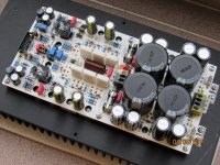
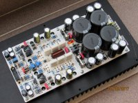
The new version of class AB buffer is finished. It's capable of working with mosfet or bjt output transistors. Furthermore, it can be configured for Class A+ operation.
Output power for the mosfet version is around 170-180W/4R, distortion in whole audio band is less than 0.01% ( 0 - 170W/4R). It's quite fast, 200ns rise time.
I will have some pcb (10-14 pcs, FR4 2x70um ENIG) for sale, just for experienced builders, requires very accurate work.
Output power for the mosfet version is around 170-180W/4R, distortion in whole audio band is less than 0.01% ( 0 - 170W/4R). It's quite fast, 200ns rise time.
I will have some pcb (10-14 pcs, FR4 2x70um ENIG) for sale, just for experienced builders, requires very accurate work.
Attachments
Last edited:
Nice Work!!!The new version of class AB buffer is finished. It's capable of working with mosfet or bjt output transistors. Furthermore, it can be configured for Class A+ operation.
Output power for the mosfet version is around 170-180W/4R, distortion in whole audio band is less than 0.01% ( 0 - 170W/4R). It's quite fast, 200ns rise time.
I will have some pcb (10-14 pcs, FR4 2x70um ENIG) for sale, just for experienced builders, requires very accurate work.
I like this very much!😎
Nice Work!!!
I like this very much!😎
thanks, some other info can be found here https://goo.gl/photos/u8XUTqYwusRXoBoD9
Very nice project. I think that you could improve CFA IPS, using current conveyor perhaps.
I see that you used asymmetric approach for mosfet OPS source resistor with the same value I used.
The PCB build looks very professional.
Any listening impressions?
I see that you used asymmetric approach for mosfet OPS source resistor with the same value I used.
The PCB build looks very professional.
Any listening impressions?
Last edited:
VFA version:
you have too many dirty signals connected to the signal ground.
I think you would do better with a dirty Power Ground, a less dirty Power Ground and a dedicated Signal Ground.
Only the input signals, NFB & servo connect to the Signal Ground.
Only fairly low AC (interference) currents connect to the less dirty power ground.
The really high AC (interference) currents from the output Zobel, the Speaker Return and the Supply rail decoupling connect to the dirty power ground.
T11 seems to be running at quite a low current (3.5mA?) would there be any benefits in moving up to 6mA or even 9mA?
I do like the non-inverting DC servo with the three stages of filtering to remove virtually all of the audio and interference signals from the -IN input.
I wonder if C4 could benefit from being direct across the Zener and instead be on the output with a 220r between Zener and cap. A much more effective noise filter.
Have you explained the difference between the two operating options lifted and grounded?
Last edited:
Believe me, hum and noise are not a concern in that case, the measured SNR is better than 90 dBV (ref 1V). Front-ends are fed from regulated power supply (located on K200v3 pcb) with PSRR 75dB. K6v2 itself has 55dB, K4v3 +PSRR 90dB and -PSRR 110dB. By the way, front-ends operate in "class A", the overall current drawing is about 20-30mA with little variation (full wave).
T11 - yes, the current is about 4mA. In this version I did not want to use heatsinks for T11,15,16,17. Previous version had heatsinks and 8mA idle current (simulations and measurements did not show real differences).
T11 - yes, the current is about 4mA. In this version I did not want to use heatsinks for T11,15,16,17. Previous version had heatsinks and 8mA idle current (simulations and measurements did not show real differences).
VFA version:
you have too many dirty signals connected to the signal ground.
I think you would do better with a dirty Power Ground, a less dirty Power Ground and a dedicated Signal Ground.
Only the input signals, NFB & servo connect to the Signal Ground.
If I did not use regulated power supply for the front-end, it might be a problem.
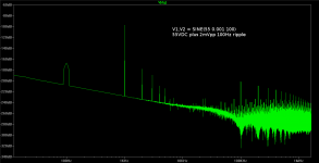
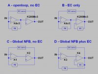
In simulation you can see two versions of power supply, unregulated SINE(55 1 100), regulated SINE(55 0.001 100) and corresponding voltage outputs at node DG. (front-end output is 1kHz sin 80Vpp)
If you have better PS by 60dB, you get better response by 60dB, that's all 😀
Attachments
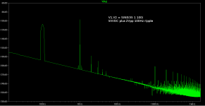
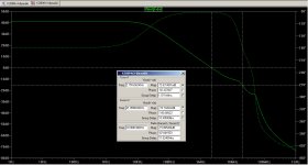
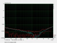
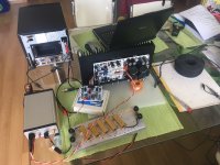
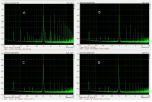
I'm going to publish some thd measurements
first of all, this is the sound card loopback at 0dBV and -6dBV (there is mess at 10k and above, maybe noise from htpc)
ASUS STX II, OS Windows 10, 24bit 96kHz, ARTA, bandwidth 20kHz
first of all, this is the sound card loopback at 0dBV and -6dBV (there is mess at 10k and above, maybe noise from htpc)
ASUS STX II, OS Windows 10, 24bit 96kHz, ARTA, bandwidth 20kHz
Attachments
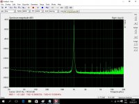
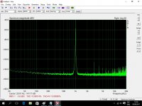
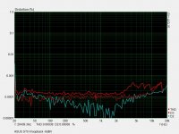

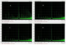
components:
* K200Mv3 (180W@4R mosfet buffer, EC, 3x IRFP240/9240)
* K4v3 (blameless based frontend, TMC compensation)
* HTPC, ARTA software, ARTA box
* ASUS STX II, WDM drivers
* 50W 4R5 resistor
conditions:
* output power 50W@4R5 (15Vrms)
* soundcard input level -6dBV (atteunation 30dB, voltage divider 15k/470R)
* floating ground, no enclosure (higher 50Hz and its harmonics)
Attachments
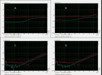
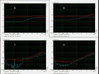
I can't make sense of the distortions being shown.
The pic for D shows 2nd @ ~-118dB and 5th @ ~-120 3rd, 4th &7th are lower and the others much lower.
The THD is stated as 0.00045% (4.5ppm)
This tallies with the sum of the peaks.
But the next grapgh showing THD vs Freq shows the total distortion @1kHz @ ~0.005% (50ppm)
It appears to me that there is a discrepancy of >20dB (10times)
OOPS. scrub that comparison, the right hand graph THD vs Freq shows 0.0005% (5ppm) - It's comparable.
It would be intetesting to see a simple IMD test spectrum, givivg, say, 14+15 KHz signals to the input at -6db level each (comparing to the level you used for single-signal THD test).
It would be intetesting to see a simple IMD test spectrum, givivg, say, 14+15 KHz signals to the input at -6db level each (comparing to the level you used for single-signal THD test).
This is not a good idea, I mean two signals at -6dBV (sound card input voltage divider is untouched), it will give 400W peak, beyond clipping. Each output signal level (13k and 14k) must be lowered by 3dB to get average power level 50W.
It would be intetesting to see a simple IMD test spectrum, givivg, say, 14+15 KHz signals to the input at -6db level each (comparing to the level you used for single-signal THD test).
he did say -6dB level comparing to level you used.This is not a good idea, I mean two signals at -6dBV (sound card input voltage divider is untouched), it will give 400W peak, beyond clipping. Each output signal level (13k and 14k) must be lowered by 3dB to get average power level 50W.

- Home
- Amplifiers
- Solid State
- HEC amp