
I was in a chat with DHL today re my lateral fet and PCB shipments - they have advised the driver of the open hours for my company's shipping/receiving department, but that hasn't seemed to keep the driver from showing up egregiously late anyway - fingers crossed,, but I'm not optimistic I'll be getting anything but excuses today...
The half-wits at DHL screwed up again and showed up almost an hour after my company's shipping and receiving had closed up shop at 1700hrs.
I will not be sparing with criticism, and will point out that our foreign subsidiaries often use DHL to send time sensitive customer problems to the home office for resolution. Since they cannot be on time to deliver, I will be recommending that our foreign offices not use DSL, as their time-sensitive issues will end up in limbo...
I will not be sparing with criticism, and will point out that our foreign subsidiaries often use DHL to send time sensitive customer problems to the home office for resolution. Since they cannot be on time to deliver, I will be recommending that our foreign offices not use DSL, as their time-sensitive issues will end up in limbo...
Last edited:
I looks like I will have to spend my lunch time to drag my sorry behind to a DHL service office to pick up the packages that they can't be bothered to deliver. Next time I deal with Profusion and PCBway, I will absolutely have to specify another carrier.
I finally picked up both my Exicon lateral fets and two sets of boards, one of them the cap board for this project. I ran around in the dark like a headless chicken trying to find the DHL service center - they don't do anything customer friendly like posting a sign. After passing by the location back & forth 3-4 times I happened to notice a gathering of DHL trucks a little bit down an unmarked driveway. Even that wasn't enough, as I had to flag down a security guard to help me find the service center. I don't think I'm going to a schedule a shipment with DHL ever again.
Ok, one of the things I have done with this revival of the Half-Nelson amplifier was to understand how things actually worked and to place provisions in the schematic so that people could get the design to work adequately with parts they actually have rather than the ideal (and not necessarily accurate) models present in various simulation software packages. The original design uses an inner feedback loop around the output N-channel mosfet and jfet driver to sim a triode characteristic. I have found that that inner loop may need some compensation for optimal performance. I have a set of boards coming in the post that has the optimization components necessary for proper performance incorporated. The new design also has a p-channel bias stage with partial bypassing so that the user can optimize the overall gain independent of what devices are on hand. It was a simple design to start with, and I think I got lucky early in the game by being able to boost the gain and output power without running into significant issues. Hopefully, the new design will make it possible to optimize given parts that are actually available. The performance of this amplifier at Burning Amp using Bill Berndt's superlative system gave me the inspiration to continue this effort.


One of the things I have noticed with this design is that the parts that were available in 2007 when I started this effort aren't necessarily the same (even given the same part number) as the ones that can be had at this late date. I was lucky back then, but lucky doesn't necessarily cut it in the engineering world.
Thank you for the kind wordsOk, one of the things I have done with this revival of the Half-Nelson amplifier was to understand how things actually worked and to place provisions in the schematic so that people could get the design to work adequately with parts they actually have rather than the ideal (and not necessarily accurate) models present in various simulation software packages. The original design uses an inner feedback loop around the output N-channel mosfet and jfet driver to sim a triode characteristic. I have found that that inner loop may need some compensation for optimal performance. I have a set of boards coming in the post that has the optimization components necessary for proper performance incorporated. The new design also has a p-channel bias stage with partial bypassing so that the user can optimize the overall gain independent of what devices are on hand. It was a simple design to start with, and I think I got lucky early in the game by being able to boost the gain and output power without running into significant issues. Hopefully, the new design will make it possible to optimize given parts that are actually available. The performance of this amplifier at Burning Amp using Bill Berndt's superlative system gave me the inspiration to continue this effort.
Here's the current version of the Half Nelson I'll be trying to optimize. One of the thing's I'll probably try is varying R7 to adjust the balance of bottom side vs. top side drive. I will also try some compensation across R20 to try and clean up some overshoot at the output that occurs when testing the amp using square wave drive.
Attachments
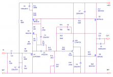
What I have done with the current version of the Half-Nelson is to decouple AC gain from topside DC bias and to allow equalization of topside and bottom side drive levels. The sum of R10 and R11 defines the topside DC bias. The bypass cap C6 allows independent setting of topside gain. Resistor R7 sets the drive level for the bottom side. I hope to be able to fiddle with these values to equalize topside vs. bottom side drive, using the voltage across resistors R17 and R22 as indications for topside and bottom side current levels.
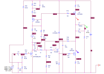
This is what things look like in sim. The actual boards are a little different, as my IRF9510 bias fets are different than the sim models. The output FETs are biasing up to around 1.25A on the bench, and I have some heat sinks that will respond nicely to some gentle airflow from a dialed-down 48V DC fan.
Attachments

Last edited:
Well, I'm still trying to discover what I did to get the original Half Nelson to work in the first place. The first incarnation came up and ran without a whole lot of difficulty, and I was able to increase the VCC for higher power output. Having said that, I had to run the original version using a lab supply before I came up with the idea of using a capacitance multiplier to make the VCC ripple go away. The trouble started when I subbed a 2SK117 for the PN4393 used in the original circuit - that one sounded like crap. I would be happy just to re-create the original circuit, perhaps with a lower capacitance depletion mode FET to sub for the original DN2540N5. I started out using an LM317 as a current source, for chrissakes...
Last edited:
I don't see those in your last schematic shown in post 94.DN2540N5 ... LM317
Also, what would be wrong with those parts? Capacitance??
Yes the DN2540N5 has significantly higher capacitance (300 pF) than the depletion mode FET I intend to use (120pF). My intended FET is the IXYS/Littelfuse IXTP02N50D, running at 20 mA, which is well within its rated IDSS.

Ah, ok DN2540 as CCS load. Yes, lower gate capaciance can be nice, but it's not everything. See here: Post in thread 'Open Source DHT Estat Headphone Amp -- OSDEHA' https://www.diyaudio.com/community/...stat-headphone-amp-osdeha.407679/post-7716964
- Home
- Amplifiers
- Pass Labs
- Half-Nelson Amp