Cut all the grounding wires that go back to the PSU.
Draw in ALL the twisted pairs that run between the modules.
Draw in the two twisted triplets between PSU and the active modules.
Now look carefully at what you have and compare to the theoretical SCH. What voltage reference connections are missing? Insert them/it
Then read D.Joffe to see where the loop current attenuating resistors need to go without increasing the interference voltage superimposed on the wanted audio signal.
This same problem occurs in ALL multichannel amplifiers. Only mono block topology avoids the loops.
Hi Andrew,
If I understand correctly, D. Joffe suggests to introduce a series resistance of 10 ohms in the signal reference cable that goes from pre-amp to power amplifier. I may have misunderstood the concept, I dont know..
......I am trying to draw a sketch as per your suggestion above.
reg
prasi
No.Hi Andrew,
If I understand correctly, D. Joffe suggests to introduce a series resistance of 10 ohms in the signal reference cable that goes from pre-amp to power amplifier. I may have misunderstood the concept, I dont know..
......I am trying to draw a sketch as per your suggestion above.
reg
prasi
D.Joffe introduces HBRL and HBRR (one in each channel) into the voltage reference links between the Signal circuits and the Power circuit. This link carries virtually no signal current but potentially carries interference currents. The resistor attenuates the interference currents, but has virtually no effect on the signal currents in the other circuits.
I don't have Joffe open, are HBRR and HBRL the correct labels for the added resistors?
No.
D.Joffe introduces HBRL and HBRR (one in each channel) into the voltage reference links between the Signal circuits and the Power circuit. This link carries virtually no signal current but potentially carries interference currents. The resistor attenuates the interference currents, but has virtually no effect on the signal currents in the other circuits.
I don't have Joffe open, are HBRR and HBRL the correct labels for the added resistors?
And the truth shall set you free!...
So here it goes. All cables and patch works created to connect power voltage reference lines to the common ground point will have some internal resistances and this in turn will induce some voltage in the signal reference lines and hence current, which in turn is amplified by the circuits. HBRR and HBRL greatly reduce the current through these wires and hence no hum.
Practical implementation?
resistance in series with left and right signal reference lines before each module that has signal in connections and has common ground point for power and signal.
Hope I got it right this time
thanks Andrew for your patience in guiding me.
Thanks and regards,🙂
Prasi
A 1-10 OHM resistor is placed between the AGND (input, feedback) and PGND (power, zobel, speaker) of every amplifier channel. You can place two in your power-amp and two in the pre-amp.
It may well be impossible to modify the boards. Can you post photo's and supply info on the boards?
It may well be impossible to modify the boards. Can you post photo's and supply info on the boards?
A 1-10 OHM resistor is placed between the AGND (input, feedback) and PGND (power, zobel, speaker) of every amplifier channel. You can place two in your power-amp and two in the pre-amp.
It may well be impossible to modify the boards. Can you post photo's and supply info on the boards?
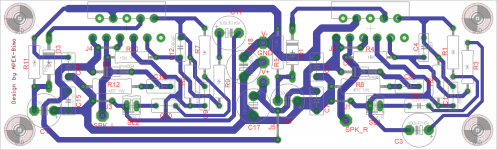
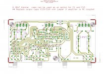
Hi Mark,
Here is the layout of example amplifier . It is designed by APEX and layout by Bimo. The resistors can be placed inplace of jumpers J3 and J1, which connect the signal ground to power ground. The example is just to understand the concept (the "D. Joffe" concept of HBRL and HBRR as given by Andrew) and can be applied to any circuit.
regards
Prasi
Attachments
Replacing J1 and J3 with 1 Ohm resistors should work. You will have placed resistors between the three ground connections of the board.
You could also add a Ground Loop Breaker (GLB) between the PSU GND and Chassis.
You could also add a Ground Loop Breaker (GLB) between the PSU GND and Chassis.
There is a Safety issue when using double insulated (ClassII) along with Earth protected (ClassI) equipment.
ClassI equipment has all exposed conductive parts connected to the Mains Protective Earth (PE).
ClassII equipment has no PE and thus cannot connect any exposed conductive parts to Earth.
These ClassII products rely on the double insulation to protect the users whenever the equipment goes faulty.
Now use a copper wire connection from a ClassII source product to the input of a ClassI Receiver.
HBRR or HBRL will stand between a Fault in the Source and the PE through the Receiver.
If the fault is a catastrophic mains to internal components short inside the ClassII equipment, then that mains voltage will be imposed ACROSS HBRR or HBRL.
HBRR and HBRL must have inverse parallel power diodes to pass FAULT Current to PE.
The route from Receiver input to PE must be robust enough to survive long enough to blow the mains fuse inside the faulty ClassII equipment.
Mixing ClassI and ClassII equipment has this hidden and fortunately very rare danger that is rarely discussed !
Hi Mark/Andrew,Replacing J1 and J3 with 1 Ohm resistors should work. You will have placed resistors between the three ground connections of the board.
You could also add a Ground Loop Breaker (GLB) between the PSU GND and Chassis.
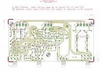
Thanks for the suggestion. Here is a version of pre-amp PCB along with schematic that I have made for a pre-amp tone control. I am not able to decide on exactly where to place the resistors. can you guide? The PCB is already made and thats when I started getting the hum...
Referring to the schematic , should HBR be placed between the grounds of audio schematic on left and supply schematic on the right?
reg
prasi
Attachments
Last edited:
Because your sch is using the general Gnd symbol it is difficult to identify the actual INPUT circuit and the actual POWER circuit.
Draw those two circuits on your PCB layout.
Check that the TWO circuits do not SHARE a common trace.
Then compare to your sch and find which trace links the Input Circuit to the Power Circuit and to the Output/Speaker Circuit.
It is this linking trace that creates the loop and needs the added resistor.
Last edited:
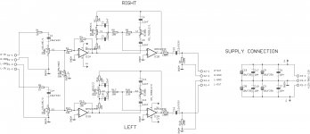
referring to the schematic, If I understand correctly, every ground on the right of IC1A and IC1B can be considered as speaker circuit and power circuit (as per Joffe terminology). Am I right in my interpretation?
reg
Prasi
reg
Prasi
I think you have that right.
Now draw out the circuits and see if they share any traces.
Then put in the in to out link/reference.
Now draw out the circuits and see if they share any traces.
Then put in the in to out link/reference.
I think you have that right.
Now draw out the circuits and see if they share any traces.
Then put in the in to out link/reference.
Ok here it goes. the schematic- GNDA is the audio return reference and GND is the speaker and power return reference. the board is also modified to to include the HBRL and HBRR in the trace between GNDA and GND.
One doubt, is it correct to join the traces for the output reference and the power reference at the power terminal (sort of output star ground)?
reg
prasi
Attachments

pins 3&5 of IC1 are connected to GNDA
pins 3&5 of IC2 are connected to GND.
That does not seem right to me.
I have never tried to build a tone control.
pins 3&5 of IC2 are connected to GND.
That does not seem right to me.
I have never tried to build a tone control.
Last edited:
pins 3&5 of IC1 are connected to GNDA
pins 3&5 of IC2 are connected to GND.
That does not seem right to me.
I have never tried to build a tone control.
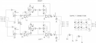
ok. Now pin 3 and 5 of both IC's connected to GNDA. How does an op-amp take reference for supply voltage? is it from pin 3 and 5? that's the big question. What about reference for audio if that's the case?😕😕😕
reg
prasi
Attachments

An opamp does not know (much) about ground. It simply tries to keep the + and - inputs at the same voltage.
Ok I did place HBRR and HBRL on amp alone and tested with sub x-over pre-amplifier that I have. Now there is no high frequency noise on speaker (which was present even when volume is muted). However when I increase the volume there is that AC hum which is volume dependent. Guess I will have to place a Ground loop breaker as Mark suggested.
Regards
Prasi
Regards
Prasi
- Status
- Not open for further replies.
- Home
- Amplifiers
- Solid State
- grounding issues with integrated amp