What are you harping on about, we don't want to create slot antennas or dipole structures on the PCB, we are talking about some basic PCB layout, talking about antennas is a lot OT.
My idea has mainly been to route an excellent single layer board (which causes me troubles with no end), and then use a ground pour for the bottom layer. As I understand, if your ground plane is connected to only one node, so no currents can be forced through it, then it can only short out fields it intercepts, and cannot retransmit any of that energy. To me that means that a ground plane with only 1 connection to the rest of the circuit cannot in any way be worse than the same circuit without the ground plane. But the requirement of only 1 connection is very strict.
Of course, I could just be ignorant.
That's more an electrostatic screen, a 0V return plane (ground plane) is exactly that it provides the return path for any signal so all device ground connections are connected to it.
Henry Ott does have some info on having a plane like you have below signals, it has some advantages for EMC and noise I will dig the relevant stuff out. It is a techniques that I have seen used on some automotive boards, hi spec for racing and some instrumentation where screening is required, these were all multilayer boards with a standard ground plane.
What are you harping on about, we don't want to create slot antennas or dipole structures on the PCB, we are talking about some basic PCB layout, talking about antennas is a lot OT.
Exactly, we do not want any such antennae, therefore we want to avoid any structures that make one e.g. slots in ground planes. It helps to understand what an (slot) antenna is made of and that if works by the theory of separating forward from the return path. You can choose to look at the material I provided and you would realize that.
@keantoken
As long as there are no loops. No multiple returns. Also from what I think I know, the highest current return closest to the star point. My pours have pads that the return goes around, but with a pour inches wide, I've had excellent results. If you do your traces and pours on the same side, you may have to look closely at it and decide where to place the boundaries so that there are no big loops. In other words, small spaces where appropriate between the same pour so that the signals travel like water finding a river, or branches to a root.
As long as there are no loops. No multiple returns. Also from what I think I know, the highest current return closest to the star point. My pours have pads that the return goes around, but with a pour inches wide, I've had excellent results. If you do your traces and pours on the same side, you may have to look closely at it and decide where to place the boundaries so that there are no big loops. In other words, small spaces where appropriate between the same pour so that the signals travel like water finding a river, or branches to a root.
Exactly, we do not want any such antennae, therefore we want to avoid any structures that make one e.g. slots in ground planes. It helps to understand what an (slot) antenna is made of and that if works by the theory of separating forward from the return path. You can choose to look at the material I provided and you would realize that.
I have read the material you posted, I have read Henry Ott's dipoles for dummies, I have read numerous tomes on this, we are arguing the same point, you can get a far more PCB design based guide by either searching for "slots in ground planes" or "return path discontinuity's" it's far easier for those of us not well versed in RF to understand, that's all I'm saying.😀
Oh by the way its an interesting read, it does show nicely how the extended return current flow can create a transmitting structure, nicely compliments the EMC stuff, as EMC is mostly RF.
Let me add this part one for those of us less into RF theory, myself included...
http://www.hottconsultants.com/pdf_files/dipoles-1.pdf
The other parts are available, I have the book, its appendix D if I remember correctly.
Let me add this part one for those of us less into RF theory, myself included...
http://www.hottconsultants.com/pdf_files/dipoles-1.pdf
The other parts are available, I have the book, its appendix D if I remember correctly.
Last edited:
@marce
I am glad you looked at the material and that we are on the same page. 🙂
I wish others would pick up on this subject.
I routinely work with multilayer RF boards, some are kW RF amplifiers, so I look at things now in a totally different way than I ever did before. The RF board material is quite expensive and if I fail to place a return path (e.g. Ground) via in the right spot it can spoil my bosses day 😀
Anyway, I don't want to harp or argue anything, but to highlight that all these (antenna, loop area, field cancellation ect.) things "mesh" with each-other and what the layout designer needs to be aware of and so he can avoid potential -got ya's....😕
No one needs to become an RF expert in antenna theory, but a tiny little peek at it does not hurt. After-all an audio amplifier is not a static DC object.
It's great that people figure out current mirrors, compute a couple equations and can run a spice simulator but this RF stuff is a whole academic level higher than that. Lots and Lots of headaches 😀
Some of the basic RF concepts, such as solid ground plane layers, once understood can be applied successfully to audio amplifier as well. This is what I am trying to make a point for.
As convenient as it is to have a double sided board with two potential routing layers, sadly we can use only one layer while having a solid ground plane layer.
As keantoken already highlighted, with respect to audio amps and double sided boards, one should make all efforts to route on one layer only by clever and sensible arrangement of components to have the other layer reserved as solid ground plane. When the ground plane layer is connected at a single point no DC currents can flow through it but due to capacitive coupling to the routed traces above, AC return currents can flow and so we allowed them not to get separated, we maintained the (current) path of least impedance and all is good.🙂
Of course the advanced layout designer can make exceptions and very cleverly use both layers for routing and as ground plane. However that is a little more tricky to do but is a valid option. Ground pours / Ground flooding and Ground stitching vias will then be used in a sensible matter. However only few layout designs shared here on the forum I have seen that done. No doubt these designers have gained the insight and experience to design well layed out circuit boards that perform without the headaches of oscillation, EMI, noise ect., they are likely working as professionals in the electronics industry.
It looks fun this PCB design stuff, must give it a go, throw a few components down and join the dots, sounds right up my street.😀
It looks fun this PCB design stuff, must give it a go, throw a few components down and join the dots, sounds right up my street.😀
I just joined the dots on a USB audio mixer.
On power up with input shorted I was getting 1VAC hum on the output !
Turned out I had mixed in power supply return wit haudio return and charging impulses into smoothing capacitors were modulating the audio return and causing massive hum.
I reworked the pcb with the power supply return kept separate and everything was fine. Star grounding is vital in audio.
Controversial 😉
That's my experience.
Without it my designs are very noisy.
I tend to use star grounding with a copper pour connected to "GND" to protect low level audio signals.
Last edited:
It looks fun this PCB design stuff, must give it a go, throw a few components down and join the dots, sounds right up my street.😀
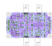
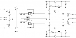
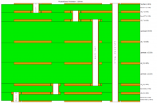
so how about this one? for a candidate?
Cap Mx by keantoken... The upstream regulator by someone else... wonder if its interesting enough..
Attachments
Nah to simple... I prefer something a bit more complex, a few hundred components, a few thousand connections, some analogue, some digital 8 to 14 layers or more😀
I was being rather tongue in cheek, with that post. (CID+ 😉)
I was being rather tongue in cheek, with that post. (CID+ 😉)
Maybe for you, but I reckon most who visit this thread are not already professionals and are looking for something to start out on.
I think we have already touched upon the most basic and simple use of a ground plane (or perhaps shield would be more accurate).
This distills down to:
1: Good grounding and routing on upper layers. You are using a layout that is ALREADY good.
2: Ground plane at bottom layer, connected to the circuit at a single point (star ground usually) and nowhere else. Bottom layer so that component pins don't create vertical loops through the ground plane.
This is a good entry point because as far as I can tell, there is nothing to lose by this approach for most audio circuitry - the ground plane only carries self-induction currents and so cannot retransmit to another area of the board. Exceptions would include places where the ground plane creates too much stray capacitance to a node, but that is unlikely.
I can think of some additional things that might be an improvement. For instance, decoupling of board input grounds to the ground plane through a capacitor. In theory this allows EHF signals to skin across the ground plane and not get demodulated in the circuit. For this reason I have actually considered connecting the ground plane at signal input shield instead of star ground, to maximize EHF skinning.
I think we have already touched upon the most basic and simple use of a ground plane (or perhaps shield would be more accurate).
As keantoken already highlighted, with respect to audio amps and double sided boards, one should make all efforts to route on one layer only by clever and sensible arrangement of components to have the other layer reserved as solid ground plane. When the ground plane layer is connected at a single point no DC currents can flow through it but due to capacitive coupling to the routed traces above, AC return currents can flow and so we allowed them not to get separated, we maintained the (current) path of least impedance and all is good.🙂
This distills down to:
1: Good grounding and routing on upper layers. You are using a layout that is ALREADY good.
2: Ground plane at bottom layer, connected to the circuit at a single point (star ground usually) and nowhere else. Bottom layer so that component pins don't create vertical loops through the ground plane.
This is a good entry point because as far as I can tell, there is nothing to lose by this approach for most audio circuitry - the ground plane only carries self-induction currents and so cannot retransmit to another area of the board. Exceptions would include places where the ground plane creates too much stray capacitance to a node, but that is unlikely.
I can think of some additional things that might be an improvement. For instance, decoupling of board input grounds to the ground plane through a capacitor. In theory this allows EHF signals to skin across the ground plane and not get demodulated in the circuit. For this reason I have actually considered connecting the ground plane at signal input shield instead of star ground, to maximize EHF skinning.
Many thanks for all of friends on forum about this debate. At the end I finally found some reasonable and eatable information about creating PCB in DIY style, all previous debate were landing on the moon with no sense. Many times I am testing 10R up resistor for lifting signal ground, sometimes go, sometimes absolutely no go and I am pushed to use star ground for qualified result. In my PCB's there is every time option for both variant. If anyone are willing, I can send him some test PCB' for ultra low noise discrete High End best quality passive 2-step RIAA (MC_MM with code switches), 3-way active Linkwitz type analog filters (100;1500; upper) or power amplifier or sharing my experiences.
Maybe for you, but I reckon most who visit this thread are not already professionals and are looking for something to start out on.
I was not being serious hence the smileys.
I did post some info regarding power amp layout and ground planes earlier, stuff that is pretty standard on many boards that have both low level signals and an amplified output. i have often given help regarding PCB design on this forum over the last 10 years and done several layouts for people when I have had the time.
I do take PCB design seriously hence the CID+.
🙂Marc
How about someone(s) sharing some examples of Successful designs to give those like myself at a Visual lesson in this exotic art form.
Thanks
Thanks
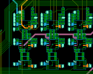
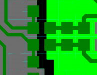
The first problem is what do you want a design off?
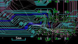
Here is a snap shot of a bit of analogue, a noise barrier, HF, and a snap shot through a layer stack for a HDI design so all the signal integrity stuff can be calculated.
Every design is different every design has solutions.
Here is a snap shot of a bit of analogue, a noise barrier, HF, and a snap shot through a layer stack for a HDI design so all the signal integrity stuff can be calculated.
Every design is different every design has solutions.
Attachments

@ keantoken, marce
I'd say PCB layout is indeed an Art. Drafting a pretty looking connection from A to B by a draftsman or just searching for a convenient way to get from A to B is no longer enough in today's world. The PCB designer must develop a habit of thinking about every single signal return path when laying down a trace or changing routing layers.
This can be overwhelming for a hobbyist who does occasional layouts for his project. (Occasionally) laying out a board without some introduction to the world of high speed signal flow, altho most say audio does not qualify as high speed, which is perhaps only partly true, makes it twice as hard for the hobbyist to come up with something that will not be a wonderful broadband ECM jammer and actually work well in the application of audio.
Sadly, even some very well seasoned designers still have trouble wrapping there heads around the PCB AC return path and stubbornly refuse to accept the solid ground plane concept as a viable concept when applied to audio amplifiers even in light of overwhelming supporting data.
Some PCB routing jobs I have done in my professional career are to most audio enthusiasts and designers weird, strange, nonsensical connections someone could possibly think of. Sure if one would use a trusty DMM and rings through some traces on one of these -weird strangers-, it be a dead short across the entire board. Yet at higher frequency e.g. 3GHz, this formerly known dead DC short has become a fine RF power combiner when terminated with 50 Ohm loads at the appropriate locations.
just my 2 cent
- Home
- Amplifiers
- Solid State
- Ground plane PCB design for power amps