...Is that 35degrees of phase margin at around 500kHz?
Will that phase dip affect the audio performance?
Basic feedback theory prediction is that the closed loop linear response has Less Error at frequencies where the loop gain is higher due to the 2-pole compensation - the response more closely follows the feedback gain setting
Yes, uS settling details will be different with the 2-pole compensation having overshoot, “long tail” settling – but way beyond audio frequencies – I see no reason to believe that such high, near Mhz time, frequency response details are relevant to audio perception
recording and playback overwhelmingly uses less than 20-~40KHz 2nd order low pass response transducers (that means 4th order low pass for the audio signal chain, musical instrument-mic-speaker-ear), digital source has Zero content over fs/2, and beyond 100 KHz air has significant attenuation
Reports of uS interaural time difference detection Are Not evidence of 100s of KHz sounds being perceived – people seem to forget that correlation at lower bandwidth with good S/N easily gives that sort of “time”/phase resolution
A practical limit to applying even higher order loop gain response is nonlinear stability
instability requires both gain and phase conditions to be met, low phase margin where the loop gain is high isn't a problem for linear system operation
the difficulty comes in nonlinear behavior - clipping effectively reduces gain and depending on system details may not change the phase much - then the low phase margin may show up as complicated clipping recovery with sticking or ringing/oscillation bursts
the nonlinear behavior may be improved by clamping diodes and other "nonlinear compensation" tricks - although 2-pole response with ~30 degrees "lower" phase margin may not be problematic
Last edited:
Anyway, one should not limit everything to audioband frequencies only. Though groundplanes have issues in power amp PCBs, they bring quiet background and RFI protection in link level stages. Neither simulators, nor THD/IMD reveal this. Real life counts.
I would worry about the 7-8 MHz loop gain intercept - particularly with BJT outputs
ideally we would like to know/control gain/phase for at least another decade - this does require RF layout technique and accounting for package lead inductance, parasitic C from heatsink mounting, wire/trace mutual coupling, ect.
chassis/pcb/output RF signal and "gnd" paths may look very different from the simple circuit schematic
in principle these can be modeled in Spice but calculating values and verifying with measurement the actual higher frequency details isn't easy and usually skipped in favor of conservative design and copying other "working" circuits
mostly we just build and hope to fix obvious problems in the prototype with Cu tape, ferrite beads, RF caps and pushing/twisting the wire harness
Planes are near and dear to me. Rule-of-thumb for
a trace very near a plane is to cut the inductance by 10.
Thus using 1nanoHenry/2millimeter for a wire in freespace,
or 12.5 nH/inch, placing that 1/16th over a plane brings you
down to 1.25nH/inch.
A key task in designing planes is to DESIGN THE PLANE.
Sketch out the various current consumers (transistors and ICs)
and sketch the arriving (+Vdd, -Vdd) currents, and then
sketch the exiting (Ground?) currents.
Use slits in the GND plane to prevent interaction, or
use heavy local bypassing+FerriteBeads to establish
a LocalBattery (copywrited phrase?). With a LocalBattery,
the only energy in the Gnd plane is DC.
just some thoughts
where should high current gnds and low current gnds be connected?
I am trying to build car chip amplifier but I couldn't decide the arrengements of GNDs.
I really didn't understand this concept.
Qestion:
Soon or later these High current gnds will meet with the low current ones.Same contamine will occur??
Probably it needs measurement but I want to ask anyway:
1-High current gnds connected to main supply bypass cap with a pcb track.
and Small current gnds connected to that track with narrow tracks(I saw p2p designs connects low current gnds to High current gnds with a resistor..Maybe narrow track take this resistor duty..?) I don't know exactly..
2-Two ground plane(one For High gnds one For low gnds).
. High current gnds plane connected to pcb dc input negative pole.
. And Low current gnds plane connected to High current gnd plane with a narrow short pcb track..
Question: Which gnd configuration may be better??
Can you give a little bit info about this?
I don't have any engineer background..
Groundplane PCB design for power amplifiers is not easy. The issue is that high currents find the way of minimum resistance through the groundplane, and contaminate low level signals by EMI. I have tried several times to design power amplifier PCBs with groundplanes, and alway got worse suppression of line frequency components than with a conventional design. Groundplanes are superb for preamps, but IMO tricky for power amplifiers.
I am trying to build car chip amplifier but I couldn't decide the arrengements of GNDs.
I really didn't understand this concept.
Qestion:
Soon or later these High current gnds will meet with the low current ones.Same contamine will occur??
Probably it needs measurement but I want to ask anyway:
1-High current gnds connected to main supply bypass cap with a pcb track.
and Small current gnds connected to that track with narrow tracks(I saw p2p designs connects low current gnds to High current gnds with a resistor..Maybe narrow track take this resistor duty..?) I don't know exactly..
2-Two ground plane(one For High gnds one For low gnds).
. High current gnds plane connected to pcb dc input negative pole.
. And Low current gnds plane connected to High current gnd plane with a narrow short pcb track..
Question: Which gnd configuration may be better??
Can you give a little bit info about this?
I don't have any engineer background..
Best: high current trace and low current trace on one side of PCB; high current ground and low current ground on other side PCB following respectively high and low path then we talking about returns for NF. Star for both path.
This is very tricky to layout but a good start.
You can also take a look how it's achieved in tube amps: high current power and separatly low current paths; separatly high current and low current ground returns, all stared.
JP
This is very tricky to layout but a good start.
You can also take a look how it's achieved in tube amps: high current power and separatly low current paths; separatly high current and low current ground returns, all stared.
JP
....Soon or later these High current gnds will meet with the low current ones.Same contamine will occur??....
We have roads with heavy gravel trucks.
We have roads that children walk along.
In an ideal town, these roads are separate. However you can't have roads that do not connect at all. So the "nice" road connects to the "load" road at one point where there are few heavy trucks. (If they connect at two points, some trucks will take the "nice" road and crush the children.)
Thanks For heavy gravel trucks & children comparison..easy to think 🙂
But
What happens when children pass narrow track(a resistor) before connected to truck way?Children turn to a truck? 🙂 or give to The children some kind of protection against trucks?
I am dead serious man 🙂
But
What happens when children pass narrow track(a resistor) before connected to truck way?Children turn to a truck? 🙂 or give to The children some kind of protection against trucks?
I am dead serious man 🙂
I use planes everywhere I can..
If I get pedantic, I create ground planes on both sides of a 2 sided and connect them with a fake part, or jumper, so that on the side with the greatest free space (usually the top since I try to run all traces on the bottom), I run my real ground plane on the top connected to the main ground net, then I create a second fake ground for the bottom, (since the traces break it up) and use a jumper to connect them near the main lug, or I disable the debugging right before I make the gerbers and violate the net rule by running a trace from that second fake ground to the main lug (star). This way, the plane on the bottom connects to no pins except the jumper, or star point.
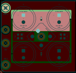
In the attached images, on the amp, you can see that I use planes for power rails, ground and pre-zobel etc.. The star
The power supply stacks and matches the connections. I try to run the power planes from one side through the filter capacitor pins to the other side, using the top for the dirty, and the bottom for the clean (filtered). Originally I tried to use the lug at the bridge rectifier as the star point, however, physically in this particular design it most likely wont be possible. So the lug to the speaker is my star point.
One of the best aspects of planes, or pours, is that if you design them well, you can simply drop parts into them and have nearly nothing to route.
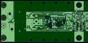
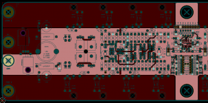
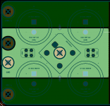
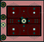


synonymous;
When I choose to use two dc supply entry(For each chip/channel), I can use The all bottom layer as a ground.
Think two square gnd plane side by side(one For low current grounds other High gnds).
And power entry on the one side of High current gnd plane.
What is the Best point(narrow track) place to Connect these gnd planes??
Can you suggest something??
What is the Best point(narrow track) place to Connect these gnd planes??
Can you suggest something??
In the center most likely
center center
bottom center
top center
In my design, I am using separate power supplies. The difference for me is that the majority of the current will be at the speaker lug and power supply ground for each side. In this case, there is no real 'star' point for me, simply the plane itself crossing the board. There aught not to be much current at all passing across this plane however seeing how each side creates it's own chaos. With the DAC located in the center, I am not at all concerned about loops or other ground issues to the point of separating them either by digital/analog, nor by high vs low current devices. Everything towards the center of the boards will be low,, with their respective grounds at the edge on the lug, where the highest currents will be.
For you, since you are using 3 separate planes, just make sure that there's not multiple paths of return within each plane to the point 'star', and keep it as short as possible. Least impedance. Technically, you could use the corners of the board as the 'through via' points for connecting your planes to the main ground plane. Planes inherently have very low impedance, so for the most part you cannot go far from best.
When two separate planes need to be connected to create a common reference, you need to determine whether any current can pass between the planes. It could be a signal current or an interference current.
Once you know that current you should determine the loop/circuit around which it flows. When you have that information you can make the informed decision on the location of the connection point to minimise the loop area of that inter-plane current.
Once you know that current you should determine the loop/circuit around which it flows. When you have that information you can make the informed decision on the location of the connection point to minimise the loop area of that inter-plane current.
Groundplane PCB design for power amplifiers is not easy. The issue is that high currents find the way of minimum resistance through the groundplane, and contaminate low level signals by EMI.
I always use a combination of ground plane and star grounding.
I put star grounds on layer 1 and ground plane on layer 2 to keep them separate. I star ground any power signals like the zobel ground and smoothing capacitor grounds. The ground plane helps protect any low level audio signals.
Hi AndrewT,
What do you think about intersection angle of ground tracks?
Let's say we have a point(circular area) that 3 gnd tracks meet.
One is power supply gnd..
Let's say other grounds low/high current gnds..
Is there anything about that in The literature?
What do you think about intersection angle of ground tracks?
Let's say we have a point(circular area) that 3 gnd tracks meet.
One is power supply gnd..
Let's say other grounds low/high current gnds..
Is there anything about that in The literature?
The Signal Return trace does not get diverted to meet up with the Speaker Return trace.
Calling them grounds when they are actually the return route for a current that is returning to it's source is causing confusion.
Stop it.
Calling them grounds when they are actually the return route for a current that is returning to it's source is causing confusion.
Stop it.
Hello all.
As some of you have become aware through my recent posts, I have become interested in sucking all the bandwidth I can out of power amps using alternate stability compensation schemes.
Do you want to build a pirate radio station?
For THD improvement a better way maybe is a system where loop gains falls with 12dB / octave or even with 18 dB/octave before the unity gain crossover.
Many modern opamps use this approach.
Today i would be temped to use digital linearization methods. You could correct the nonlinearity of our amp in the digital domain.
I'm sure this is old hat for many of you been-there-done-that guys, but looking at wiring parasitics in the simulator I realized that low-inductance traces are probably necessary to implement alternate compensation with adequate phase margin for stability.
I doubt that. A 10 cm line has about 100 nH Inductance or about 4 Ohm at
1 Mhz.
And inductance can improve stability as it has a positive phase shift.
1: For a balanced line, the magnetic fields of the signal flowing in opposite directions cancel out and result in lower inductance as long as the conductors are close enough.
The magnetic field of the two wires superimpose in a positive way according to the "right hand rule".
2: For a single conductor close to a conductive plane (IE a ground plane), the magnetic field produced by the signal will cause eddy currents in the plane with opposing magnetic fields, again canceling inductance depending on the distance to and quality of the plane.
Eddy current play no role at frequencies below 10 MHz with 35 um thick
groundplanes.
Inductance can not be cancelled out. This is property of geometry. The
inductance of a loop is proportional to the area of the loop.
The whole magic of a ground plane is that you keep the current loop small.
At audio you have to worry a lot of the resistive coupling you introduce with a ground plane.
I can understand that calling "return path" For other gnds rather than power gnds.
I think because of that they have different potential..
But my question remain same:
Why some p2p designs use a RESISTOR to Connect the low Level signal returns to power gnd??
How do you determine this resistor Value?
Same question with different way:
Why some p2p designs use different Cable thickness to Connect to star Point?(I am not talking about Cable should need to be necessary thickness to pass current..).I saw they are especially Using very thin wires For low Level signal return..
On pcb Design is there any simplified rule For intersection angle between power gnd track and signal return tracks?
There's a series of articles on the TI website that you may be interested in..
http://www.ti.com/lit/an/slyt499/slyt499.pdf
http://www.ti.com/lit/an/slyt512/slyt512.pdf
Some thorough literature if you look around some
http://www.ti.com/lit/an/slyt499/slyt499.pdf
http://www.ti.com/lit/an/slyt512/slyt512.pdf
Some thorough literature if you look around some
- Home
- Amplifiers
- Solid State
- Ground plane PCB design for power amps