For example, at 2.83V output (1W into 8 ohms), a VAS with 80dB gain will have an input signal of only 283 uV. Of course GNFB will "correct" this noise and the math eventually "works out" but this does make me somewhat uneasy
I ran some sims on a conventional, Self AB and found that with a power supply of 36V, 1KHz input of 360mVp and 14.14Vp output into 8R there were some interesting results.
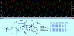
With a video transistor as VAS (C3423) and usual common emitter configuration the drive is a combination of both voltage and current, see attached.
Red is the output voltage waveform (+20dB into 8R 1KHz), green is the current variation at the base of the VAS, and dark blue which is the voltage variation at the base of the VAS and very small, as you suggest. I have attached that waveform for the VAS voltage and it is far from linear; it is clear the negative feedback is working well to make this amp pretty linear.
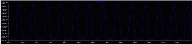
If you examine the current range at this output it is 22uA to 38uA - VERY small, and the voltage changes are 425mV - from -35.268V to -34.846V.
With such drive voltages and currents, reflecting the complex math of the base/collector transfer, you would expect noise. The only way to improve these results and BTW improve speed by reducing parasitics, would be to drive the VAS at the emitter in grounded base. But that is very low impedance, high drive, and not always easy to arrange.
Attachments
That's actually not that bad, compare it with my circuit, at the base of the beta-enhancer.
😱
Edit: That's at 40 Vp, imagine at 4Vp
😱
Edit: That's at 40 Vp, imagine at 4Vp
Attachments

Last edited:
19/20 kHz IMD .Instead of the ne5534 should LM101/153UD2. Broken-chain OOS gain 100 dB at 20 kHz
Attachments
Last edited:
At over 10 MHz unity loop gain that's going to be a challenging layout.
Also you want to simulate loop gain with different DC offsets. Pick a DC offset that causes the output stage to conduct around 1 to 2 amps into the load. Then do a loop gain plot and check gain margin.
Also you want to simulate loop gain with different DC offsets. Pick a DC offset that causes the output stage to conduct around 1 to 2 amps into the load. Then do a loop gain plot and check gain margin.
Finally something interesting. I've been experimenting with some circuit lately and loading the VAS with particular value resistor, lowered the 2nd harmonic quite a bit...
Hello
What value of resistor are you using to load the vas ?
Myself I use a 17 k ohm resistor load in my amps vas
Thank
Bye
Gaetan
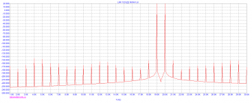
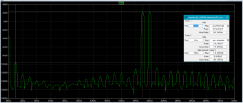
Here is the CCIF 19+20k IMD at 80 Vpp into 4 ohms, and loop gain plot. I cut off the IPS from the amp image since it is based on Figure 7.13 in Bob Cordell's book, not sure if I'm allowed to post it here.
I can't see the 1kHz difference spur, which normally is the whole point of the 19+20kH.
Jan
I can't see the 1kHz difference spur, which normally is the whole point of the 19+20kH.
Jan
Looks like the frequency axis labeling got messed up, it's there at -96 dB (-119 dB below 19 kHz component).
Attached is the fixed chart.
Attachments
Finally something interesting. I've been experimenting with some circuit lately and loading the VAS with particular value resistor, lowered the 2nd harmonic quite a bit...
Just a FWIW, the 2nd is relatively innocuous and can mask higher ordered harmonics. But you'll know you're really making progress when the higher orders (5th and above) are reduced (the higher the better that it be reduced) as the ear is far more sensitive to the higher orders. The ear converts all forms of distortion into some kind of tonality- and because the ear uses the higher ordered harmonics to sense sound pressure it has to be keenly sensitive to them! The higher ordered harmonics thus contribute to brightness and harshness.
If you are using a 100Hz test signal, pay attention to harmonics between 3KHz and 8KHz. But also use a 1KHz test signal and look at the 5KHz to 12KHz region- if you get good reductions there that's really what you are looking for.
Has this ever existed?Good points. I think it is extremely rare to see an amp without ANY sort of feedback. It can be hidden as local emitter degeneration, or the positive feedback involved in cascoding and bootstrapping, or whatever, but I have yet to see one with no feedback at all.
Jan
How would an effective output stage be possible at all without some form?
High gain stages + step down transformers or something like that... maybe more plausible with tubes?
relevant
Last edited:
(time for edit ran out)
So just to add that , however small, some inherent device feedback is inescapable, but the amount can still be controlled just like global feedback.
So just to add that , however small, some inherent device feedback is inescapable, but the amount can still be controlled just like global feedback.
maybe more plausible with tubes?
These arguments always devolve into semantics. Yes, you can have a SS o/p stage free of local or global nfb but the devices are used as followers which implies a 100% voltage nfb. Similarly with tubes. Being triodes, they are inherently based on nfb, so pedantically, no topology based on triodes can ever be nfb free.
For the purposes of sanity, single stage vs multi stage nfb seems more useful.
Is a Vbe multiplier negative feedback ? How about a BJT with Collector connected to Base ? Is thermal feedback negative feedback ? How about short circuit protection ?
Cathode biasing of a Common Cathode Triode is negative feedback, but if you put a big capacitor across the resistor, the signal doesn't see the feedback. Do we really need to count DC feedback as negative feedback ?
How about a differential pair ? If you only feed signal to one side, does the emitter or source impedance of the other side count as negative feedback ?
I like to think of negative feedback as feedback that affects the signal's amplitude and THD, not the DC operating point of a circuit.
Yes, you can have a SS o/p stage free of local or global nfb but the devices are used as followers which implies a 100% voltage nfb.
The question was about not using any form of feedback, including degenerative feedback, in an output stage/follower (in theory).
You can have a common collector with no external emitter resistor providing a lot of gain with next to no feedback, then you can have a transformer on the output.
There is probably some basic principle that I'm missing in this example e.g like input impedance decreasing or output impedance increasing roughly proportional to gain or, more obviously, how terribly it would perform, but this is a very simple example anyway... Jan seemed to imply it was at least not impossible.
You guys need to stop confusing equilibrium with NFB. Otherwise everything is a NFB device including a resistor. 😎
Member
Joined 2009
Paid Member
I’m very positive about feedback!
LOL, that can get you into 'big oscillator' trouble!
Hi Jan, All,
What about this? https://www.diyaudio.com/forums/solid-state/347482-seen-rush-pairs.html#post6030076
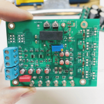
Here's a 100W build. RHS is PA, LHS is driver with soft clip....It can be used as a no feedback amplifier with current drive output.
No local or global feedback and it sounds OK with reasonable sensitivity speakers.>=90dB/W/m..
Attachments
Last edited:
- Home
- Amplifiers
- Solid State
- Global Feedback - A huge benefit for audio