Many of you are familiar with The Class-A Amplifier Site (TCAAS), now hosted as part of Rod Elliott's ESP website (Elliott Sound Products - The Audio Pages (Main Index)). Geoff Moss is the creator of the TCAAS and was of great help to me when I built my version of the JLH. I built the amp in 2005 and it has been my main amplifier ever since, driving the midrange/tweeter in a biamped system.
I have not communicated with Geoff for several years now, and he has not been active on diyaudio for about the same period (his health was deteriorating at the time). With the continued interest in the JLH, I thought it would be good to post the PCB design files that Geoff gave me. I have had several enquiries over the years and at least one forum member (Mamak) has built a version.
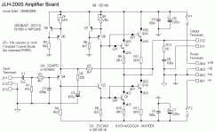
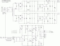
The design is based on the schematic "Fig 3 The Higher Power Circuit" on the "JLH Class-A Update" page at
The Class-A Amplifier Site - JLH Class-A Update
(with the addition of a "Zobel network" on the output).
Rod has placed Geoff's design files including schematics and PCB fabrication files on the main TCAAS page:
The Class-A Amplifier Site
with a link having the heading
Geoff Moss Construction Information
This provides a zip file with the various required files and more background information from both Geoff and myself.
I highly recommend that any who are interested read the entire article "JLH Class-A Update" that explains the modifications to the original JLH design.
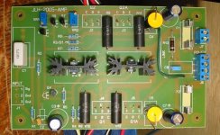
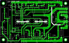
Schematic and picture of my completed PCB are attached.
By the way, if you have not already done so, I recommend checking out the rest of Rod's ESP website. There is an incredible amount of design information at this site, for all levels of audience. Thanks Rod!
I have not communicated with Geoff for several years now, and he has not been active on diyaudio for about the same period (his health was deteriorating at the time). With the continued interest in the JLH, I thought it would be good to post the PCB design files that Geoff gave me. I have had several enquiries over the years and at least one forum member (Mamak) has built a version.
The design is based on the schematic "Fig 3 The Higher Power Circuit" on the "JLH Class-A Update" page at
The Class-A Amplifier Site - JLH Class-A Update
(with the addition of a "Zobel network" on the output).
Rod has placed Geoff's design files including schematics and PCB fabrication files on the main TCAAS page:
The Class-A Amplifier Site
with a link having the heading
Geoff Moss Construction Information
This provides a zip file with the various required files and more background information from both Geoff and myself.
I highly recommend that any who are interested read the entire article "JLH Class-A Update" that explains the modifications to the original JLH design.
Schematic and picture of my completed PCB are attached.
By the way, if you have not already done so, I recommend checking out the rest of Rod's ESP website. There is an incredible amount of design information at this site, for all levels of audience. Thanks Rod!
Attachments
That is very kind of you.
But PCB shops these days charge essentially the same for 1 or 2 layer 35µm copper.
They charge a lot more for 70µm, even single layer.
Would it not be an idea to duplicate the power tracks on the top layer for better conductivity ?
Cheers,
Patrick
But PCB shops these days charge essentially the same for 1 or 2 layer 35µm copper.
They charge a lot more for 70µm, even single layer.
Would it not be an idea to duplicate the power tracks on the top layer for better conductivity ?
Cheers,
Patrick
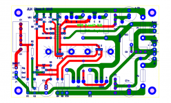
As I noted, Geoff Moss did this layout. I have no way to modify it. I just posted the Gerbers so others could have it built.
Yes, somebody could certainly create a top layer to add parallel tracks by editing the bottom layer. One of the free Gerber tools would probably work for this.
Yes, somebody could certainly create a top layer to add parallel tracks by editing the bottom layer. One of the free Gerber tools would probably work for this.
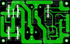
Yes, I did not build the Power supply PCB so Geoff did not generate Gerbers for me. My power supply has huge capacitors and Geoff thought I did not need a capacitance multiplier. I made one for another project and just handwired it.
I tried to import the Gerber files and the drill later in the given link above.
But I had no success with multiple software for Gerber viewing.
I did manage to load the Gerber files into a CAD software.
As a tribute to Geoff Moss, I decided to refresh those Gerber files and the drill files.
Hopefully they could be more compatible to today’s PCB shop settings.
I tried my best not to change anything, including layout, component placement, etc.
But there are a couple of changes which I consider beneficial.
1) The high current tracks are repeated on both top and bottom layer.
This not only double the copper cross-section, but also the surface area.
2) The pins of all TO92 devices are placed on a triangle and marked with E,B,C,
so that devices with different pin assignments can still be used (e.g. BD560, KSA992, 2SA970BL, ….., etc.)
3) Some signal tracks running parallel to neighbouring ones are moved to the top layer to reduce cross coupling.
4) The power devices in the original layout are TO3 metal case, remotely connected to the PCB by flying leads.
The revised PCB has a minor revision to allow the direct soldering of TO247 or TO3P devices onto the PCB.
TO3 metal case can still be wired with flying leads without problems.
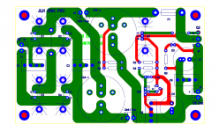
To complete refreshing Geoff’s work, I also made a set of Gerber files for his power supply PCB.
Unfortunately, no Gerber files are available.
So I had to import the graphics image of the PCB and trace that with a CAD software.
The position of components might not be accurate to the last 0.1mm.
But I hope I have been able to retain the original overall layout.
The enhancement changes mentioned above have also been implemented on the PSU PCB.
Hopefully someone skilled in PCB layout can double checked my revision before realising them in hardware.
I find it very difficult to find my own mistakes, but it is quite likely that there might be some.
My highest respect to Geoff for his exceptional work which makes thing easy for all of us.
Patrick
.
But I had no success with multiple software for Gerber viewing.
I did manage to load the Gerber files into a CAD software.
As a tribute to Geoff Moss, I decided to refresh those Gerber files and the drill files.
Hopefully they could be more compatible to today’s PCB shop settings.
I tried my best not to change anything, including layout, component placement, etc.
But there are a couple of changes which I consider beneficial.
1) The high current tracks are repeated on both top and bottom layer.
This not only double the copper cross-section, but also the surface area.
2) The pins of all TO92 devices are placed on a triangle and marked with E,B,C,
so that devices with different pin assignments can still be used (e.g. BD560, KSA992, 2SA970BL, ….., etc.)
3) Some signal tracks running parallel to neighbouring ones are moved to the top layer to reduce cross coupling.
4) The power devices in the original layout are TO3 metal case, remotely connected to the PCB by flying leads.
The revised PCB has a minor revision to allow the direct soldering of TO247 or TO3P devices onto the PCB.
TO3 metal case can still be wired with flying leads without problems.
To complete refreshing Geoff’s work, I also made a set of Gerber files for his power supply PCB.
Unfortunately, no Gerber files are available.
So I had to import the graphics image of the PCB and trace that with a CAD software.
The position of components might not be accurate to the last 0.1mm.
But I hope I have been able to retain the original overall layout.
The enhancement changes mentioned above have also been implemented on the PSU PCB.
Hopefully someone skilled in PCB layout can double checked my revision before realising them in hardware.
I find it very difficult to find my own mistakes, but it is quite likely that there might be some.
My highest respect to Geoff for his exceptional work which makes thing easy for all of us.
Patrick
.
Attachments
That's pretty awesome, Patrick. I will load a Gerber viewer and have a look at your files.
I'd consider asking Rod to replace the old with your new files (or maybe include both), but it would be nice to know first that somebody has used the files successfully.
I'd consider asking Rod to replace the old with your new files (or maybe include both), but it would be nice to know first that somebody has used the files successfully.
Just wish to pay respect to Joh Linsley Hood and Goeff Moss for their contribution to DIY.
Patrick
Patrick
PaulB & EUVL,
This is absolutely brilliant, thank you. I have been meaning to build this amp for quite a while now. I have the heatsinks packed into a cupboard, and was going to get around to this project eventually. I even bought Cadock 0r1 resistors as per the original layout.
This will help to get this done a lot quicker now. I'll just be using MJ802s instead of the 15003s as I have a whole bunch of them. I also have a whole bunch of caps and CRC PSU boards.
Kevin
P.S. I also have some CapMX PCBs to try as well
I downloaded Viewmate and had a quick look at your revised files - they seem fine to me. Well, better in fact. Are you by chance a professional PCB designer?
You had me a bit worried, but Viewmate had no problems in loading Geoff's original files. So I don't have to ask Rod to pull them down, thankfully.
For those thinking of building the JLH, I would go with Patrick's revisions.
You had me a bit worried, but Viewmate had no problems in loading Geoff's original files. So I don't have to ask Rod to pull them down, thankfully.
For those thinking of building the JLH, I would go with Patrick's revisions.
ferret,
I started with 2N3055s for testing but then upgraded to the MJ15003. It made quite an improvement to the sound quality.
I started with 2N3055s for testing but then upgraded to the MJ15003. It made quite an improvement to the sound quality.
The online viewers I tried would not show the drill file properly.
Also the ones I posted have top copper and bottom silk in addition.
You should consider MJW3821, KSA992, TTC004B.
They were already mentioned in the other thread.
Patrick
Also the ones I posted have top copper and bottom silk in addition.
You should consider MJW3821, KSA992, TTC004B.
They were already mentioned in the other thread.
Patrick
Here the relevant links :
JLH 10 Watt class A amplifier
JLH 10 Watt class A amplifier
JLH 10 Watt class A amplifier
Patrick
JLH 10 Watt class A amplifier
JLH 10 Watt class A amplifier
JLH 10 Watt class A amplifier
Patrick
With due respect to Geoff, I have taken the liberty to add one more comment on Geoff's layout.
Geoff has included power rail fuses on both the amplifier and the power supply PCBs.
Each of the power supply PCBs is for on rail.
So there are a total of 4 fuses.
I shall not get myself into the discussion of sound of fuses.
BUT the worse thing that can happen to a speaker is for one of the rails to fail.
This in turn will cause a huge DC offset at the amplifier output.
If the intention is to prevent current run-away, one should consider other protection circuits.
This should either isolate the speaker from the amplifier output.
And / or deactivate both rails simultaneously.
If I would use Geoff's PCBs to build, I would seriously consider bypassing the fuses.
Cheers,
Patrick
And if done with floating ground - the midpoint of the capacitors without connecting to the transformer.
We'll have to change the bias of the first transistor. Make a divider of resistors between the power rails with filtering to the midpoint.
We'll have to change the bias of the first transistor. Make a divider of resistors between the power rails with filtering to the midpoint.
Last edited:
I agree with speaker protection external to the amp. A big advantage is that I can build new amps to try out without adding speaker protection circuitry to each amp.
Mine is based on Rod Elliot's project, once again at the ESP website (A PCB is available):
Loudspeaker Protection and Muting
A word of warning: make sure you test the protection! My initial approach was to use the NTE7100 (supposedly a replacement for the UPC1237) but I found it just did not respond to DC voltages correctly. Rod's detection circuit is simple and elegant.
I very much doubt that I can hear the sound of the fuses. I see them as protecting the power supply more than the speakers.
Even a 60MHz output transistor works in this version.
I also made improvements for both CCS.
Otherwise a great amp.
https://www.diyaudio.com/forums/solid-state/3075-jlh-10-watt-class-amplifier-762.html#post6489035
I also made improvements for both CCS.
Otherwise a great amp.
https://www.diyaudio.com/forums/solid-state/3075-jlh-10-watt-class-amplifier-762.html#post6489035
- Home
- Amplifiers
- Solid State
- Geoff Moss's JLH-2005 design files