cjd said:Is this just a really low gain circuit, and mine is sounding as expected?
C
I would say no. The gain of my SuSy chipamp is actually not low at all. In fact I lowered the gain on my XBOSOZ to just 6db for driving the SuSy as I was only using the lower 1/3 of the volume control.
Ed actually had a good point, it may not be at the input into the power amp wher a lead is reversed. It could be into the input of the XBOSOZ or your JT.
Cheers!
Russ
Input of the X-BOSOZ it isn't... I- and IG both go to the outer of the RCA, I+ from the pin... I'll certainly give it a shot the other way.
JT, how the heck does it make any difference? It's just a linear pass-through on each "side" I thought. . .
At any rate, I had similar "low gain" issues with just the 100K pot as well - yes, I know there are potential issues here, could have wired this backwards as well, etc.
I could also have a PCB issue going on here, though I went over it a fw times (and found mistakes... easily corrected). however, I'll try to remember to post these when I'm on the computer that has 'em. 🙂
C
cjd said:Input of the X-BOSOZ it isn't... I- and IG both go to the outer of the RCA, I+ from the pin... I'll certainly give it a shot the other way.
JT, how the heck does it make any difference? It's just a linear pass-through on each "side" I thought. . .
At any rate, I had similar "low gain" issues with just the 100K pot as well - yes, I know there are potential issues here, could have wired this backwards as well, etc.
I could also have a PCB issue going on here, though I went over it a fw times (and found mistakes... easily corrected). however, I'll try to remember to post these when I'm on the computer that has 'em. 🙂
C
C,
What would make a difference is if you had GND connected to where the hot signal should be. It would make no difference which polarity you used for the balanced signals hot leads. But if you had a GND going where a signal should you would have a problem.
Ed and I were just saying it never hurts to check that you don't have a GND wire going to where a signal wire should be.
Cheers!
Russ
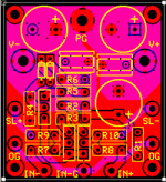
The "X" board.
Outputs to amp are pulled directly from the appropriate pins of the ZTX closest to R3 (error 1 on this PCB)
Also, R1 has been properly connected to V+ (it's floating on one end on this PCB)
And finally, I have installed 20kR between each input and G (in front of R7/R8).
I've since completely revamped this and it is (I think) much improved.
Attachments
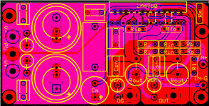
And, the LM4780 board.
one per side. Cap from the bridge board to signal input, wire from the ground out on the bridge board to IG. wire from OUT to the SL (same side as the signal to this amp board is taken) on the bridge board, and to one terminal of the speaker.
OG is ignored/unused, and R1 is not filled.
This board layout has also been revised, such that it can now take two discrete inputs and have separate outs, OR can have one input to both and the outputs joined back up to create a parallel setup.
I will have to verify that I have properly connected I- and IG on the X-BOSOZ together, with I+ correctly connected to the signal (pin) on the RCA jack.
Past that, I do not believe that it should make any difference at all how consecutive parts are wired, as long as signal is always to signal, and ground is always to ground.
Given that I got similarly "quiet" results without the X-BOSOZ or JT in the picture, my suspicion is on the bridge board or the amplifier board. I will have to go back and triple-check that I installed all the parts in the right places, just to be sure. But, again given that I have the same problem with both LM3886 and LM4780 boards in the picture... 🙂
C
Attachments
Russ,
I got a few quick moments, so I thought I'd better reply to the question you asked me in a private e-mail, regarding adding a cap across the CCS diodes. The answer is that adding a cap certainly couldn't hurt, although I haven't noticed that adding one made a significant difference. If you choose to add one, my calcs say that 1uF should be more than enough, as the diode noise in this case tends to be in the upper frequency range. A nice little polypropylene film cap ought to do the trick very nicely indeed.
cjd,
The circuit gain of the last version update I posted in this thread was a hair short of 30dB.
Cheers,
Terry
So, I am listening to my prototype right now (same boards and parets as Russ). My temporary PS is 4 MUR820s and a bank of 4 Nich 12k 35V caps. The only (somewhat) suitable trafo I have on hand is a 160VA(!) 22V, which is actually about 25V unloaded. Under power, my rails fall to about 30-31V, which is still a bit high but fine for testing.
Even with this limited supply, and driven SE directly from a Sony CDP (variable outputs), the sound is very impressive. Lots of detail and, well, power. Can;t comment on imaging etc, as I'm just powering my bench speakers at the moment. The CDP only goes down to -20dB, so I can only play it loud and louder 😉
Very excited! Ordering some big trafos now...
Terry,
Thanks for the validation. I have already added a diode bypass cap to the PCB. 🙂
All,
a note about DC offset on the input of the amp. The latest design posted by Terry has a DC offset of around 1.8-2.0 V on each input (+ and -). The can have nasty effects on some pots and attenuators (crackles, pops, and dead pots sometimes) so a good input cap would be a great idea. Somthing like a 10uf 250V Solen MKP would work great.
Cheers!
Russ
I have been really busy with stuff for the SuSy chiamp.
Some of you may be interested in this:
http://www.diyaudio.com/forums/showthread.php?s=&threadid=79930
Some of you may be interested in this:
http://www.diyaudio.com/forums/showthread.php?s=&threadid=79930
 I can not figure out why mine is so quiet. I tried swapping leads into the X-BOSOZ and no change in output at all. I must have a resistor in the wrong place somewhere or something - at least I was consistent about it! 🙂 I tried swapping leads into the X-BOSOZ and no change in output at all.
The sound is great otherwise.
If we put more monster caps on the input, will we need the smaller value caps that have so far been used between the transistors and the chip-amps?
Been tapping holes lately, and not much else. 😉 Loads of fun, you know?
C
Tapping holes
You may be aware of this already.
I use a VSR drill with a clutch for tapping holes. I chuck the tap in the drill. The clutch allows setting the max torque to avoid breaking the tap. The variable speed allows some touch in the process and reverse relieves the manual labor invloved. Keep a small gage wire brush handy for clearing chips. Don't forget the eye protection.
Been tapping holes lately, and not much else. Loads of fun, you know?
You may be aware of this already.
I use a VSR drill with a clutch for tapping holes. I chuck the tap in the drill. The clutch allows setting the max torque to avoid breaking the tap. The variable speed allows some touch in the process and reverse relieves the manual labor invloved. Keep a small gage wire brush handy for clearing chips. Don't forget the eye protection.
Well, I've verified all the component values. So I am at a loss on why things are so quiet. On the parallel amp, I *am* finding that, of course, many resistor values are about half since they're all ultimately "shared" at the input - not sure if that makes much difference for the circuit stability. I've tested with the 3886 as well as the 4780 though, and both are quiet.
Ed: good tip! A bit nervous about trying that just 'cause of the leverage involved, but...
C
Ed: good tip! A bit nervous about trying that just 'cause of the leverage involved, but...
C
Some more musings
A while back it was proposed that the THS4131 and its family might work fine for this application, and Nelson seemed to agree that it should.
I am thinking this could be the answer to a couple of key questions I have.
Terry's circuit sounds absolutely fantastic, but I think it would sound even better without the feedback cap or an input cap. Unfortunately you seem to really need both.
So I did a little digging and came up with this, which is very similar to what I had seen earlier.
I have plugged in values for the resistors, but I am not at all sure they are sane. I would sure like some feedback from you all as to if they look like they will work, or if they could be better.
I am shooting for a voltage gain from the circuit of ~22X.
Areas of concern....
1) Are R7 and R8 values too high? Just seems like a high value for a current feedback opamp to me. Is it OK? Will CMRR suffer?
2) R3.,R4 and R5/R6 are there to isolate any parasitic capacitance from the THS4131 and give the non-inverting input of the LM3886 a GND reference. Am I on the right track including them, and are the values OK?
Here is the schematic as a PDF.
Thanks!
Russ
Attachments
Russ,
First off, great to see you continue the initiative in this area, and a good start so far. I (finally) got a chance to look at your idea a little closer, and I agree with your thoughts that R1 through R8 will need some adjustment.
Let me start by commenting on R3 - R6. For the values you posted, I am pretty certain the circuit will be unstable.
In my (non-THS4131) circuit, I had about 150dB open loop gain, threw away about 25dB of gain with the voltage divider network, leaving approximately 94dB of feedback to produce 29dB gain closed loop. Any more feedback and the circuit stability went to H E double hockey sticks (a Canadian pun for the devil's abode).
The THS4131 has 90dB open loop gain, and the LM3886 has 115dB open loop gain, for a total of 205dB open loop gain for your circuit. Your closed loop gain is about 27dB, and you aren't throwing any gain away, so your feedback is 178dB. Because the THS4131 is an IC and is also unity gain stable, you can probably get away with more feedback than the 94dB limit of my circuit, but I doubt it will let you go that far. Also, the LM3886 likes a bit of impedance feeding its input, around 10k-20k. So, I would suggest a starting point for prototyping would involve throwing away around 20 dB of gain, with R3|R4 = 10K, and R5|R6 = 1K.
On the input side of things, the datasheet for the THS4131 tells two different stories. In one area they say the input capacitance is only 4pF and the input resistance is 34Mohms, which indicates that relatively high resistance values would work for R, R2, R7, and R8, but on page 19 there is a table that indicates R1 and R2 should be around 400R, and R7 and R8 should be around 4K, then on page 6, Figure 1 they show a value for R7,8 of 4K. A bit of a hodge podge going on.
Based on what I see in the datasheets, I think (if it were my decision) I might use R1|R2 = 500R, and R7|R8 = 10K. That should still leave the input impedance somewhere around 20-30K, and give the circuit good performance.
I'l wrap my suggestions up with the statement that when I was developing my circuit using the ZTX450 input transistors, it took me about 30 or so iterations of trial and error trying different resistor values to find workable values for the input, divider, and feedback resistors. So don't be discouraged if it takes some time to find the right combination. I think you are on the right track to finding the newer improved GC Supersymmetry circuit.
Cheers,
Terry
metalman said:Russ,
I think you are on the right track to finding the newer improved GC Supersymmetry circuit.
Cheers,
Terry
Terry,
First off, just want to say thanks you are a great guy.
I would really doubt many would say your circuit reall "needs" anything if they could only hear it. It really is superb.
I just personally would like to get rid of the signal path caps if I can. I really appreciate your comments here and now I understand better why you made some of the choices you did. The old light bulb went off. 🙂
I will plug in your values and see what I get. But as far as far as the circuit goes it does not appear anything is missing at least(I hope). Just some value need to be arranged. 🙂
I will post an updated schematic here soon.
Cheers!
Russ
Trying to do my homework....
Ok So I have done some quick calculations lets see if I am way off...
Lets assume 1V input.
The input is attenuated to .1V(1K/10K) then amplified by a ratio of 23.1 to 2.31V by the LM3886 which is then applied to the opposing input of the THS4131 which should result in a total gain ratio of 2.31 x 20 (10K/500R) giving a total cct gain ratio of roughly 46.2V, or about 33.3db.
Did I figure that out correctly? Or am I totally missing it.
Now, that seems(assuming its correctly firgured) like a wicked huge amount of gain to me. I don't need anywhere near that much. So I was thinking more along the lines of 20db.
It sems to me the easiest way to get to around 20db is to reduce R7/R8 to 2.2K which should bring it completely inline with the datasheet for the THS4131.
All of that is assuming my calculations are correct, which is no safe bet. Any thoughts, or pointers?
Thanks.
Russ
Totally ignore my previous post... its probably so far off its not even funny. Thats what I get for posting before I have had at least one beer.  Reading my book, and refiguring. I think I am at least on the right track though.
Reading my book, and refiguring. I think I am at least on the right track though.Perhaps this?
Well here is my pre-breakfast crack at the circuit. I lowered some resistor values a bit, and I put notes on the schetatic to show my train of thought. Now hopefully people can see clearly how I am calulating things and let me know if I am right or wrong. 🙂
One big question I have is how did you figure input ideance Terry? 😀 I can't seem to figure it out. It seems to me the input impedance will be 402ohms in my circuit, but you see to think it will be much higher. Can you explain briefly describe the forumla for calculating Zin on this circuit?
Cheers!
Russ
Attachments

- Home
- Amplifiers
- Pass Labs
- GC SuperSymmetry