Nelson Pass said:I have a couple more for you today, Brian. I believe they
will address some of these issues.
I don't personally know that the 3886 is better sounding than
the 3875, but I would would bet that it is based on the data
sheets: Lower open loop gain, higher bias, smoother spectral
distortion plots. I'll let you know when I've had the time to
play with them properly.
😎
Thanks for the interesting design ideas.
Another interesting option for the pcb would be to use the LM4780 (2x50w chip), and parallel both channels of it together to replace the LM3875. Hopefully this would solve the problems with low impedence loads.
As for the current layout, I realized that I accidently omitted C5 (thanks for pointing this out metalman), which I will add in there tonight.
--
Brian
Good point. I often forget that the rest of the world even
thinks about such things. Feel free to scale it X 10 or so on
the input network. Use high beta transistors if you encounter
difficulty, which I don't think you will. 😎
thinks about such things. Feel free to scale it X 10 or so on
the input network. Use high beta transistors if you encounter
difficulty, which I don't think you will. 😎
Wouldn't a 1k-ohm input be a good candidate for drive by a high-output impedance current source?
Erik
Erik
still input impedance
Mr Pass,
In your article you mentioned about the importance of bandwith up to 100khz, because lower than that audio signal will be affected in phase or magnitude.
About BOZOS. I wanted to modify it like Zen 6 or 7, putting local feedback from D to G. I calculate if the differential if pair of IRF610 (TO-220 size), also from your paper it is about 1N7 input capacitance.
If the D-G resistor is 100K and input resistor is 10K it will give local gain about 10x. But the cutting frequency for 10K+1N7 will be 9.3khz?
You suggested input buffer like Zen4, but this will be the last effort I will take.
How do you use IRF610 for hot differential, achieving local gain about 10x, having fairly high input impedance (above 3K at least), but still have bandwith 100khz?
The 610 out to fall out at about 100K with a 10K input and
a 100K feedback, if my thumbnail calculation is correct.
a 100K feedback, if my thumbnail calculation is correct.
Mr. Pass,
The calculation is not as simple as filter at 10kohm+input capacitance=1N7?
What is your thumbnail calculation?
I got all the data and knowledge from your papers. Now there is something new to combine all that?
The calculation is not as simple as filter at 10kohm+input capacitance=1N7?
What is your thumbnail calculation?
I got all the data and knowledge from your papers. Now there is something new to combine all that?
Actually I recall this being so from a previous test. If you
take the 10 pF or so of DG capacitance of the IRF610 and
compare it with the 100 Kohm of your feedback loop, you
get a pole at about 180 KHz. This will be the most imprtant
capacitance figure of the three - the GS capacitance is much
higher but doesn't see much voltage change at all.
The XA amplifiers are fine examples - they go to 100 KHz and
use 610's and a 10K input resistor.
Wow, there are things about simple 3 leg mosfet that are tobe understand more. I recall the mosfet capacitance are 3, GS, GD, DS. In your paper, one of them is multiplied by the gain factor.
Also, from designs of your 3 stages power amp (like A75), you seldom use darlington or triple darlington output stage. The VAS usually directly goes to output stages. What is your opinion about darlington or triple darlington output stages? They can reduce bias needed in VAS, but whats the "not-good" thing about them?
Mr. Pass, if I can get a hint, what is the differential CCS bias current and folded cascode current in X1000?Originally posted by lumanauw
X1000 uses TO-247 mosfet for output device. If each has 8nF input capacitance, 40 of them will have 320nF that will have to be charge-filled to achieve at least 100khz.
In folded cascode, the driving swing is equal to the swing in the differential. How to calculate how many mA needed to drive gate capacitance of final mosfets to certain output voltage at certain Khz?
I remember someone give me this formula
I=2xPixFxCxV,
where
I=current needed in Ampere
Pi=3.14
F=Frequency Hz
C=capacitance Farad
V= voltage
I calculate, if I wanted to charge all the mosfets for their Vgs (I take V=6volt), F=100khz, C=320nF, the result is 1.2A
Am I making a mistake in this calculation? Why the result is over 1 Ampere?
This is not quite right. A MOSFET's capacitance is typically characterized as: Cgs, Cgd and Cds. In a follower configuration, Vgs is almost constant, while Vgd changes quite a lot. The effect of Cgs is thus very small, and devices are typically optimized for low Cgd. Since the voltage at the drain is constant, you don't get into multiplicative effects either. I would thus base calculations on desired voltage swing (in X, half of it since it is balanced) and total Cgd + any parasitics you might want to model.
Also, please note that devices are typically characterized in terms of gate charge, and the apparrent capacitance is greatly reduced as the Vgd becomes larger.
Also, from designs of your 3 stages power amp (like A75), you seldom use darlington or triple darlington output stage. The VAS usually directly goes to output stages. What is your opinion about darlington or triple darlington output stages? They can reduce bias needed in VAS, but whats the "not-good" thing about them?
For your consideration, here is my initial attempt at implementing Nelson's circuit topology presented at the begginning of this thread. I have incorporated an additional element, which is bootstrapping the op-amps to provide greater current delivery into lower impedance loads. I have simulated it in Spice, and it appears at first glance to be stable, with the exception of signals above 200kHz.
I am hoping over the next few weeks to prototype it and see how it performs. In the meantime, any suggestions on improvements are welcome.
Terry
P.S. Sorry about the image quality, I couldn't get it too accept a larger image size.
I am hoping over the next few weeks to prototype it and see how it performs. In the meantime, any suggestions on improvements are welcome.
Terry
P.S. Sorry about the image quality, I couldn't get it too accept a larger image size.
Attachments

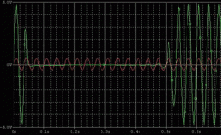
I got the results from the circuit
I tried to simulate the circuit by Pspice and found that at high frequency sinusoidal input signal (about 10k-20kHz), the result indicated me high frequency noise interfered with the input signal which I put a filter to remove it. After output signal passed that filter, that noise could be removed out from the output signal 😀. However, I found something's strange when low frequency sinusoidal signal is supplied through the circuit as below attached file.
I tried to simulate the circuit by Pspice and found that at high frequency sinusoidal input signal (about 10k-20kHz), the result indicated me high frequency noise interfered with the input signal which I put a filter to remove it. After output signal passed that filter, that noise could be removed out from the output signal 😀. However, I found something's strange when low frequency sinusoidal signal is supplied through the circuit as below attached file.
Attachments
Gencard,
Thanks for the response. I had noticed the high frequency issue, but the low frequency one I missed. I'll have to fiddle with it some more and see where it is coming from. Hmmm.......
Thanks for the response. I had noticed the high frequency issue, but the low frequency one I missed. I'll have to fiddle with it some more and see where it is coming from. Hmmm.......
Metalman,
I have no idea to solve that problem. I don't know the root cause of it. However, I will try to make the protype for listen the sound from the circuit if I have more free time to do it.
I have no idea to solve that problem. I don't know the root cause of it. However, I will try to make the protype for listen the sound from the circuit if I have more free time to do it.
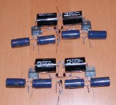
Progress, slow but certain!
Finally got around to putting something together. Have the two channels finished, now to connect up a power supply, input and output connectors.
Finally got around to putting something together. Have the two channels finished, now to connect up a power supply, input and output connectors.
- Home
- Amplifiers
- Pass Labs
- GC SuperSymmetry