You are welcome Vasilis. This time it's very quick deliver  in fact first one to out of India.
Regards
Prasi
in fact first one to out of India.Regards
Prasi
sheets updated.
CRCRC GB LIST - Google Sheets
almost all shipping are done except a few.
Today evening or tomorrow , I will share the tracking numbers.
regards
Prasi
CRCRC GB LIST - Google Sheets
almost all shipping are done except a few.
Today evening or tomorrow , I will share the tracking numbers.
regards
Prasi
I got mine too. Massive thick boards that can survive a bomb blast!
Thanks, Prasi.
The LT4320 active bridge units are very slick too.
Thanks, Prasi.
The LT4320 active bridge units are very slick too.
Thanks for confirmation x, glad you like them.
To wong,
The small PCBs are the ideal bridge rectifiers (as a gift!). The paypal invoice had the attachments, kindly save them.
I will upload them here some other time.
regards
Prasi
To wong,
The small PCBs are the ideal bridge rectifiers (as a gift!). The paypal invoice had the attachments, kindly save them.
I will upload them here some other time.
regards
Prasi
The pin spacing in the LT4320 bridges is a little different than holes for the monolithic bridge on the CRCRC - no big deal as I can bend the leg a bit as they are jumper wires. But the bridges will be more performance, less heat, and lower cost than 8 TO220 diodes, 4 SK heatsinks, and 16 film caps. Those Class A rectifiers were always a pain to setup and build.
The pin spacing in the LT4320 bridges is a little different than holes for the monolithic bridge on the CRCRC - no big deal as I can bend the leg a bit as they are jumper wires. But the bridges will be more performance, less heat, and lower cost than 8 TO220 diodes, 4 SK heatsinks, and 16 film caps. Those Class A rectifiers were always a pain to setup and build.
yes, the pin spacing on the LT4320 bridge PCB is 5.08 mm, whereas hole spacing on the CRCRC PCB its 5.33mm. Shouldn't pose a problem I guess.
yes definitely should be very easy to build and can be used on any design of the PSU.
Please note that there is a LED and resistor on the back side and also an electrolytic cap (10uf) can be soldered and made to stand above the board (like a flag). this should make it as a complete rectifier in itself and with visual indication too.
especially for CRCRC, they should be able compensate for some of the voltage dropped through the RC stages.
Boards arrives safely and look great, awesome packing, thanks Prasi!
And nice surprise photo under the flap!!
BK
And nice surprise photo under the flap!!
BK
Hi Prasi,
Did you ever post a schematic with part numbers for the active bridge? I noticed this is an 8pin SMT and different than the 12pin MSOP package I used. DFNs are a bit trickier to solder as there are no exposed leads like MSOP. Just confirming you are specifying the LT4320xDD package? Let us know if you have a dual die n channel low Rdson MOSFET in mind. I was going to suggest the SQJQ910 as a possibility. Maybe you spec’d all of this but I must have missed it. Good call to add an indicator LED on backside and optional electrolytic. Thank you for including these as gifts with our CRCRC orders. If folks give this a try and use it instead of the bank of 8 x TO220 MUR diodes and their requisite heatsinks and caps, you will find improved voltage headroom, lower (none) switching noise, and almost no heat dissipated for a cooler running amp. Plus, overall cost is less than traditional route and it’s faster and easier to build.
Thanks,
X
Last edited:
Boards arrives safely and look great, awesome packing, thanks Prasi!
And nice surprise photo under the flap!!
BK
Thanks for the confirmation BK.
😀, the surprise photo is sent to everyone of the GB subscriber, so they know me.🙂
Hello X , thanks.Hi Prasi,
Did you ever post a schematic with part numbers for the active bridge? I noticed this is an 8pin SMT and different than the 12pin MSOP package I used. DFNs are a bit trickier to solder as there are no exposed leads like MSOP. Just confirming you are specifying the LT4320xDD package? Let us know if you have a dual die n channel low Rdson MOSFET in mind. I was going to suggest the SQJQ910 as a possibility. Maybe you spec’d all of this but I must have missed it. Good call to add an indicator LED on backside and optional electrolytic. Thank you for including these as gifts with our CRCRC orders. If folks give this a try and use it instead of the bank of 8 x TO220 MUR diodes and their requisite heatsinks and caps, you will find improved voltage headroom, lower (none) switching noise, and almost no heat dissipated for a cooler running amp. Plus, overall cost is less than traditional route and it’s faster and easier to build.
Thanks,
X
Here are the schema and BoM for both versions of the ideal bridge rectifiers.
ver1. without AC snubbers (smaller PCB- 21.5mmx30mm)
ver2. with AC snubbers (bigger PCB- 25mm X 30mm)
I was unable to include these in all the packages as I ran out of rectifier PCBs.
The BoM attached is for the rectifier with snubber components.
I had in mind , the SQJB00EP mosfet , which is will generate about 10mW/ amp more than the mosfet you suggested above. Still should work well in the design.
Regarding the LT4320 package, I have incorporated options for both DFN as well as DIP08 package. Only those who are good with smd soldering may attempt soldering DFN package.
here is an example by EEVblog guy
YouTube
regards
Prasi
Attachments
-
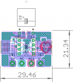 ideal bridge layout no snubber.png40.7 KB · Views: 761
 -
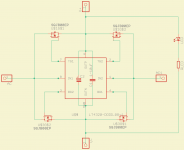 sch no snubber.png21.2 KB · Views: 13,822
 -
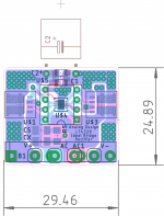 ideal bridge layout with snubber.png42.4 KB · Views: 764
 -
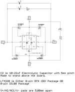 schema-ideal Bridge- with snubber.png22.2 KB · Views: 776
 -
IDEAL BRIDGE+snubberR3_ListByValues.pdf57.7 KB · Views: 304
-
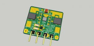 3d1.jpg119.9 KB · Views: 14,653
Last edited:
- Home
- Group Buys
- GB: CRCRC PSU