Hi. Still no reply from some GB members. I'll certainly have extra pcb, so if still interested send me a PM, and I'll put you on the waiting list. Thanks
SB
SB
Here is a link to the GB for Toshiba Jfets:
https://www.diyaudio.com/forums/gro...oshiba-2sk170-bl-grade-jfets.html#post5718262
https://www.diyaudio.com/forums/gro...oshiba-2sk170-bl-grade-jfets.html#post5718262
Here is a link to the GB for Toshiba Jfets:
https://www.diyaudio.com/forums/gro...oshiba-2sk170-bl-grade-jfets.html#post5718262
Just put myself on the list!
Algar,
Would you mind supplying the dimensions for the PCB? And if you know already, the height of the tallest capacitor would be great.
I wanted to start designing/selecting an enclosure.
Thanks!
Would you mind supplying the dimensions for the PCB? And if you know already, the height of the tallest capacitor would be great.
I wanted to start designing/selecting an enclosure.
Thanks!
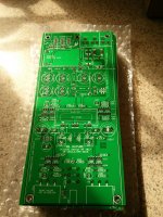
Hi. Tallest capacitor, at the most! is 40mm, if using the 1455N2201 Hammond enclosure. The PCB size, designed to fit the same enclosure is 4'' x 8.75''
PCB was shipped a few days ago, should be here within the next 1-2 weeks...
Still no reply from DontHertzMe and Tubo.
Thanks
SB
PCB was shipped a few days ago, should be here within the next 1-2 weeks...
Still no reply from DontHertzMe and Tubo.
Thanks
SB
Hello Algar_emi,
showing at your posted photo and I know its late be not too late: are you sure that main voltage creepage is safety!
JP
showing at your posted photo and I know its late be not too late: are you sure that main voltage creepage is safety!
JP
Hi. From reference I got: ''Typical FR-4 PCB will have a Dielectric Strength (or Dielectric Breakdown voltage) in the order of 10s of kilovolts per millimeter''
Therefore, running Line traces on the top layer and Neutral traces on the bottom is fine. As for the clearance, 220Vac = 313Vpk, from pcb safety table for commercial and industrial design (from SMPS design rules), coated external trace (with soldermask), minimum spacing is 0.4mm. I have 0.9mm, which is good for at least 500Vpk. Input varistor limit to max 275Vac, or 388Vpk.
Should be ok.
Just tested the power supply section under 120V and 240V and got a stable 23.92Vdc in both cases. Supply is working fine...
SB
SB
Assembled rest of the CRC filter and working fine. When assembled with all the filtering caps, this supply pack some serious juice. Even if the 10R CRC resistors will limit the current, try not to short it... Will try to assemble the rest tomorrow...
Correction for the pcb clearance, unit conversion error, I have 0.090'' spacing, not 0.9mm, that is 2.2mm. So it is rather 1KVpk, a confortable margin from 240Vac, or 340Vpk... Sorry again.
SB
SB
Hello again,
sorry if I´m pedantic but it is regarding safety.
According DIN EN 60664-1:
- 2.3mm between L and N
- 5.0mm between L an earth (FPE) and between N and earth (FPE)
JP
sorry if I´m pedantic but it is regarding safety.
According DIN EN 60664-1:
- 2.3mm between L and N
- 5.0mm between L an earth (FPE) and between N and earth (FPE)
JP
creepage on PCB. Through PCB is really not the problem then PCB is FR4.
Using EAGLE allows you to work with constrains for ERC.
JP
Using EAGLE allows you to work with constrains for ERC.
JP
I agree with you, this is not ideal. I added the ground plane under the SMPS module after one member concern that the module may radiate some RF. Then made an other change for the J113 and forgot to get back to have a closer look to the gnd plane. I agree that ideally the line traces should had been excluded from this zone, my fault...
From what I found on the net, this is not a real concern, but if you're worried, the ground plane is not grounded by default, there is provision to add a small R0805 and cap to gnd under the PCB, don't ground it if you're worried. Also as a corrective action we can always cut the PCB trace and run a short lenght of insulated wire directly to the SMPS module pin, from under the PCB, it won't show from the top.
Personnaly I'll use the board as it is. Sorry again...
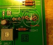
Found one error on C203 silkscreen, see picture. One '+' sign is wrong, it is in fact a GND pin. Please make sure to install C203 correctly...
From what I found on the net, this is not a real concern, but if you're worried, the ground plane is not grounded by default, there is provision to add a small R0805 and cap to gnd under the PCB, don't ground it if you're worried. Also as a corrective action we can always cut the PCB trace and run a short lenght of insulated wire directly to the SMPS module pin, from under the PCB, it won't show from the top.
Personnaly I'll use the board as it is. Sorry again...
Found one error on C203 silkscreen, see picture. One '+' sign is wrong, it is in fact a GND pin. Please make sure to install C203 correctly...
Attachments
- Home
- Group Buys
- GB B1 Nutube PCB with integrated PS