The Theta-JA (thermal resistance from junction to ambient) is ca. 175 °C/W for the ZTX558.
You can improve the cooling on E-Line or TO-92 parts with little brass clip-on heatsinks from the various distis.
What also works for me: some EMC copper tape wrapped around the case, and stuck to the PCB. Or, soldered to some separate copper sheet. Small pieces like this can get the power handling of E-Lines to 700mW, with <100 °C junction temperatures. There are no SOA complications - the 700mW can be applied at high voltage.
My initial experiment will run the transistor at 0.25W and I usually have a fan blowing across the desk and it is wintertime in the garage, so nice and cool.
Of course, experimentation might lead me to a completely different operating point or conditions. I have been looking at some of the clip-on heatsinks just in case.
It seems like the surface-mount version of the ZTX558 might also be good for pushing dissipation higher. You can build a plane with some area and I've seen boards with surface mount heatsinks like this one to get even more heat out. Edit: The FZT558 datasheet even discusses copper plane conditions for pushing it to 3W.
SOT223 558: it's tempting. The downside is that the heatsink pad is, as usual, the collector, where the Shunt Cascode output is taken. The very large voltage swing on this node is not so good to apply to a big pad, it may couple to other nodes, and raise the risk of oscillation, etc.
I did some testing today. Heater voltage was 6.23V. Grid bias was initially -1.395V and I had to keep making small adjustments every few minutes for 20 minutes or so. Bias was -1.411V at the end of the test and seemed to have stabilized somewhat. Bias for this stage is balanced on a knife's edge at any given moment. Measured gain was 2358.
Here is 22.5Vrms out:

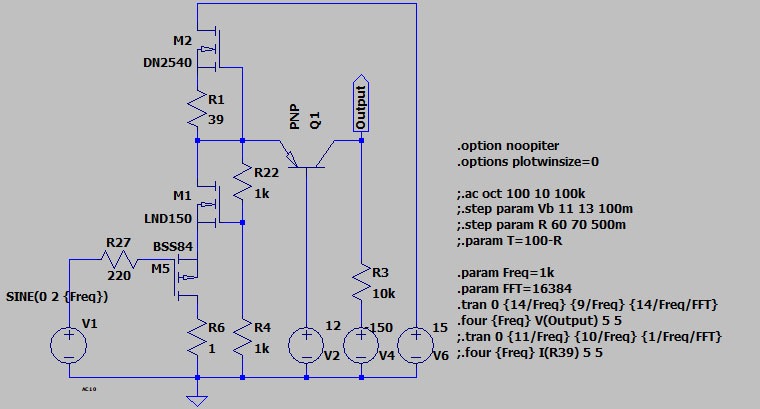
Distortion is in the noise. Unfortunately, there is a lot of noise.
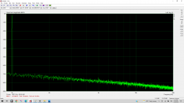
Here is 65Vrms:

Pretty low distortion.
Here is 75Vrms:

It's not clipping yet, but it is getting close.
I imagine that I need to quiet the supplies for the base voltage and the negative rail. These were just cheap 48V switching supplies stacked to make these rails. This test was just to look at harmonic distortion, and the result was quite favorable. I'll make a separate post with a summary of the distortion of the CCS-loaded 6BN11 stage that am comparing this to.
Here is 22.5Vrms out:
Distortion is in the noise. Unfortunately, there is a lot of noise.
Here is 65Vrms:
Pretty low distortion.
Here is 75Vrms:
It's not clipping yet, but it is getting close.
I imagine that I need to quiet the supplies for the base voltage and the negative rail. These were just cheap 48V switching supplies stacked to make these rails. This test was just to look at harmonic distortion, and the result was quite favorable. I'll make a separate post with a summary of the distortion of the CCS-loaded 6BN11 stage that am comparing this to.
This is 22.5Vrms and 65Vrms out for the CCS-loaded 6BN11 stage:


As you can see, much more distortion and much less noise.
As you can see, much more distortion and much less noise.
Excellent developments, very interesting to see the comparison.
Yes, the negative supply is extra-sensitive. The impedance of the neg rail also affects the output & distortion I suspect. I'm thinking about that, because of the 4.5kHz noise bump. I believe that is caused by rising impedance around that frequency due to the output LC filter of the Line→DC converter (10µH - ca. 220µF maybe?).
Yes, the negative supply is extra-sensitive. The impedance of the neg rail also affects the output & distortion I suspect. I'm thinking about that, because of the 4.5kHz noise bump. I believe that is caused by rising impedance around that frequency due to the output LC filter of the Line→DC converter (10µH - ca. 220µF maybe?).
@SpreadSpectrum : I'm looking forward to be able to perform some tests as well on some circuits, your threads are always very interesting!
@Rod Coleman : I'm playing with LTSpice and a SS version of your circuit.
It is basically an hybrid with the UNSET concept applied to triodize the n-fet curves and then your shunt cascode.
Components are not optimal for the shown voltages, because this one started from another one designed to drive tube SE stages with SS driver (that on LTSpice gives 370Vpp at 0,07% THD with 2Vrms at its input).
Adding a cap at the inlet of the circuit (needed to manage 2Vrms), what do you think about grounding the base of the PNP and refer the gain stage (normally grounded) to a negative voltage? Will this simplify the noise issue and so requirements for power supply?
On simulations, harmonics drop at -30 dB from the previous one (8th is few ppb).
Thank you in advance, sorry for the partial OT.
I was able to get a bit of time in on this project. I put some LC filters on the output of the switching supplies and got the circuit noise floor down a bit. Cleaning up the supply feeding the transistor base helped noise a lot more than cleaning up the negative rail, although both need to be clean and stable.
See attached. The combination of high gain (>65dB) and low distortion is pretty astounding. Usually, those are very difficult to put together in the same stage. I also found it interesting how little 2nd harmonic distortion is there. I expected more.
The CCS-loaded 6BN11 is currently cancelling a lot of 2nd harmonic in my Corona amplifier. 2nd is slightly lower than 3rd at some power levels. It would be interesting to see how this circuit plays in that amp.
Right now, I'm getting periodic sudden shifts in plate voltage. I suspect that the output of the switching supplies is the culprit. I don't think their output is as stable as I need it to be. Worse, it doesn't drift slowly but shifts suddenly from time to time (usually in the middle of a measurement).
Rod, how are your boards coming along? Is it something you are actively working or is it a someday project?
Attachments

The 2nd harmonic seems to be lower when a higher value of load resistor is used.
The results look very good...
Yes, the board is under active development. The schematic is complete, bar the adjustable negative regulator, but I have just received a separate board to test that, and I'm assembling it this week. It's a useful item in its own right.
The results look very good...
Yes, the board is under active development. The schematic is complete, bar the adjustable negative regulator, but I have just received a separate board to test that, and I'm assembling it this week. It's a useful item in its own right.
> what do you think about grounding the base of the PNP and refer the gain stage (normally grounded) to a negative voltage? Will this simplify the noise issue and so requirements for power supply?
I have thought about that many times, but the catch is running the signal source into an input socket that is always expected to be at 0V and connected to ground / PE. If you have a signal transformer, it's OK. But that is an expensive item, so my solution will be to regulate the supply voltages carefully, and eliminate noise that way.
I have thought about that many times, but the catch is running the signal source into an input socket that is always expected to be at 0V and connected to ground / PE. If you have a signal transformer, it's OK. But that is an expensive item, so my solution will be to regulate the supply voltages carefully, and eliminate noise that way.
Ok, I'll be in for a couple of the boards when they are complete.
The very low 2nd was surprising to me. I think if I replace the 6BN11 stage with this stage in my transmitter triode amp, I will end up with more 2nd at the output (since it seems to be mostly cancelling now) and less 3rd (since this stage has less 3rd).
The very low 2nd was surprising to me. I think if I replace the 6BN11 stage with this stage in my transmitter triode amp, I will end up with more 2nd at the output (since it seems to be mostly cancelling now) and less 3rd (since this stage has less 3rd).
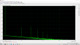
I've been mulling this over a bit in my mind. In my SE amp, I drive the cathode of the CCS-loaded 6BN11 from a p-channel fet follower. This gives me a high-impedance non-inverting input to the stage. The amplifier has significant feedback so the common mode voltage is essentially 600mVpk on the grid and cathode of the pentode. The voltage variations between the cathode and screen grid (600mVpk) are fairly insignificant for a pentode. The screen just isn't that sensitive to voltage variations of that size.
I think that common mode voltages on the grid and cathode of the 6e5p might throw this stage off more. I'm trying to logic this out from looking at characteristics but I think variations between the cathode and the cascode voltage will be more significant than they were with the pentode.
I did experiment with bootstrapping the screen to the cathode with the 6BN11. It helped distortion slightly at some power levels and made things slightly worse at others, so I left it out. Seemed to be a net zero overall.
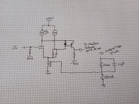
I may have to do something like that with this stage though.
Edit: added a picture to illustrate
I think that common mode voltages on the grid and cathode of the 6e5p might throw this stage off more. I'm trying to logic this out from looking at characteristics but I think variations between the cathode and the cascode voltage will be more significant than they were with the pentode.
I did experiment with bootstrapping the screen to the cathode with the 6BN11. It helped distortion slightly at some power levels and made things slightly worse at others, so I left it out. Seemed to be a net zero overall.
I may have to do something like that with this stage though.
Edit: added a picture to illustrate
Attachments
I prefer low impedance drive for the PNP's base; but I am sure you know how to check and account for this.
If the output resistor is a high value, some kind of servo for the output voltage is likely to be needed. This is the part that is catching me now. The linear servo's tradeoffs are not so easy to resolve, especially in this time of parts shortages.
If the output resistor is a high value, some kind of servo for the output voltage is likely to be needed. This is the part that is catching me now. The linear servo's tradeoffs are not so easy to resolve, especially in this time of parts shortages.
@Rod Coleman how "low" the impedande of the PNP base has to be?
If the current of the CCS on its base is 10x the base current is still acceptable even is the impedance in high?
Thanks
If the current of the CCS on its base is 10x the base current is still acceptable even is the impedance in high?
Thanks
I don't think so much about current; but the (network) impedance looking out of the base should be <100Ω for best results, as a guide. Adding an emitter follower to the CCS is one way to do it. At higher current in the output, a voltage regulator is good.
Way lower than what I'm simulating by now.
A lower driving impedance improves distortion/detail/both?
Would you reccommend in PP designs too?
A lower driving impedance improves distortion/detail/both?
Would you reccommend in PP designs too?
Adding a follower is very easy, compared to the complexity of the driver stage; I recommend adding it in all cases. In any cascode, series or shunt, the stiffness of the cascode voltage is of prime importance. Yes, you can measure it in the output spectrum.
I will be experimenting a lot with the voltage on the base. I don't want to make this any more complicated than it needs to be, so the idea is to start simple and see what effects I get from additional complexity.
I'm taking the Douglas Self approach here and evaluating not just the impact of changes on the performance of the stage, but on the performance of the whole amplifier. Any additional subsystem complexity should be justified by a system-level improvement. We'll see where the balancing act ends up.
I'm taking the Douglas Self approach here and evaluating not just the impact of changes on the performance of the stage, but on the performance of the whole amplifier. Any additional subsystem complexity should be justified by a system-level improvement. We'll see where the balancing act ends up.
Could it be the place for a LR8?
https://ww1.microchip.com/downloads/en/DeviceDoc/20005399B.pdf
Maybe with some help from T1?
![268[1].jpg](https://www.diyaudio.com/community/attachments/268-1-jpg.1053152/ "268[1].jpg")
https://ww1.microchip.com/downloads/en/DeviceDoc/20005399B.pdf
Maybe with some help from T1?
- Home
- Amplifiers
- Tubes / Valves
- Folded/Shunt Cascode driver for 211