It's OK Mark, I just need to isolate or cancel the MOSFET stage to track the problem backwards. I will not have the Zetex transistors until late next week because a Mouser package takes about 6 days to come down here. So I don't care heating the BC's transistors a little while I measure the voltages of the first stages with time enough. Then you can help me determine what the problem is. Should I swap the 2 BC's for 2N5551/5401 for this test?
In short yes...little Cu/Al heatsink wrap around TO-92 case would help to disipate heat.Should I swap the 2 BC's for 2N5551/5401 for this test?
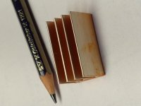
Maybe its my old eyes (or brain) but this (white looped in pic below) looks to me like it might be 12R read from one end, or 1K read from the other. If it is the R27 that I think it might be, could explain some of the excess heating in subsequent stages.
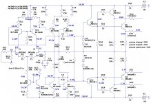
Sorry I don't remember which earlier poster to properly credit, but someone mentioned the all phase-lag compensation ... Looks like the scheme in the first of the Goldmund 330 schematics might have been what he/she meant:
- there's a 100n capacitor in parallel with R27
- remove C3, C4, C8, and C17 (each imparting phase-lag compensation)
- the new C17 is 15pF, one leg to J2-G as original, the other to Q1-Collector
The cap across R27 helps Q8 and the current mirror keep pace with Q1, which would otherwise always be faster than a sequence of 3 devices.
There will probably still be issues due to differences in output devices, but at least the Global loop might cooperate better.
You've done such a lot of fine work already -- it'll be great to get it back to making beautiful sounds.
-Best regards, Rick
Attachments
Last edited:
Oh, and if you can score some, the MPSW42(NPN)/-92(PNP) are a good fit specs-wise for the VAS devices that are running too warm - 300V, 500mA, 1W, 'tall' TO-92. The Goldmund 330 Clone posted earlier by aparatusonitus showed them. (And he gets the credit for the lag/lead compensation knowledge.) But the pinout probably won't be convenient.
Another way to save output expenses -- only place one pair -- one N-ch, one P-ch. You can even just lift the Gate lead on the other two; well, don't leave it floating - tie it to the Source to make sure it stays off. And no-load, of course!😉
-Rick
Another way to save output expenses -- only place one pair -- one N-ch, one P-ch. You can even just lift the Gate lead on the other two; well, don't leave it floating - tie it to the Source to make sure it stays off. And no-load, of course!😉
-Rick
Last edited:
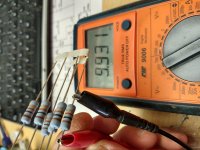
The resistor in question is certainly not 1% but 5% tolerance, as indicated by the last gold ring. The color order indicates that it is 10k resistance (brown, black, orange and gold) or 1k resistance ((brown, black, red and gold) ... should be checked with DVM.
The proposed Zetex transistors can be used with minimal fuss.
The proposed Zetex transistors can be used with minimal fuss.
Btw, i also recommended changing the value of R27 from 10k to 8k2 with the aim of equalizing the dissipation on Q1/Q8 transistors in static condition (the current through VAS and output stage remains almost unchanged).
Hello friends, well ... first things first. Today is a national holiday here so I managed with the components I have handy in my boxes.
Here are the measurements of one of the two copied amplifier boards. I will finish the second board and report today. It seems that these are normal gate values at the output. MOSFETs totally unmounted. Q1 and Q5 are now 2N5551 and 2N5401. Of course there was something wrong. These 2 transistors were 180 degrees rotated. 😱 Sorry, I did this before aparatusonitus warned me for the transistors to come ZTX658/758.
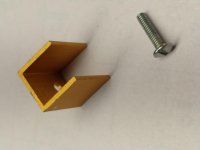
I believe that I would have to add heat sink to the future ZTX658/758 transistors, no matter their 1W dissipation characteristics, heat is there anyway, right? I should get some special heat sink for this, I don't like the epoxy solution too much.
Thank very much Rick PA Stadel and aparatusonitus for your last juicy posts. I will get back to you soon after I finish measuring the second board. This is getting very interesting, I am learning so much from you guys, thank you again for being so patient.
Here are the measurements of one of the two copied amplifier boards. I will finish the second board and report today. It seems that these are normal gate values at the output. MOSFETs totally unmounted. Q1 and Q5 are now 2N5551 and 2N5401. Of course there was something wrong. These 2 transistors were 180 degrees rotated. 😱 Sorry, I did this before aparatusonitus warned me for the transistors to come ZTX658/758.
... don't be fooled by the way pinout is shown in both datasheets!!!
I believe that I would have to add heat sink to the future ZTX658/758 transistors, no matter their 1W dissipation characteristics, heat is there anyway, right? I should get some special heat sink for this, I don't like the epoxy solution too much.
Thank very much Rick PA Stadel and aparatusonitus for your last juicy posts. I will get back to you soon after I finish measuring the second board. This is getting very interesting, I am learning so much from you guys, thank you again for being so patient.
Attachments

First let's clarify some things by referring to your last post/schematic:
1) whether or not the amplifier uses Q7/Q14 pre-diver transistors. If the answer is yes, the current through them will need to be reduced by increasing the value of R34 to approx. 560-680 Ohms or go for Zetex transistors
2) why the circuit still uses unnecessary C8/C17/C3/C4 compensation instead of a single capacitor (~15pF) from collector Q1 to gate J2
3) why the diagram still shows Q8=BC556B and Q2=BC546B when we concluded long ago that there should be at least 2N5401 and 2N5551 with heatsinks. In addition, Q2 and Q5 form a simple current mirror that must be designed with paired/match transistors of the same type.
4) Q3/Q4/Q6/Q13 driver transistors will need heatsinks anyway, whether they be Zetex or something else.
Hi aparatusonitus , yes we agreed for those changes, but in the middle I discovered 2 reversed transistors. Now I am making all the changes al least in one of the boards. I will report when ready, the board has pads so little that is suffering so careful changes take some time. We will make them all. I was preparing another post before this quick reply for you, coming next.
Hello Rick PA Stadel, thank you for your interesting comments, greetings from Buenos Aires. Checked R27 because I also have old eyes and brain, and it reads almost 10K matching the 5% tolerance as aparatusonitus says.
These 2 boards apparently are throwing the same voltages. Gate voltages seem to be more reasonable in the range of +/-0.9V to 1.1V, with the feedback trick done with 170 Ohms that I could get in my resistor box, as today I can't go get better values because of national holiday. Also R32 y R33 change their values or get open as I test and fail. I have replaced them a couple of times. This time I removed the SMDs and placed 2 matched 39 Ohms, sorry no 33 Ohms available today
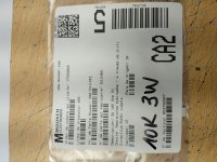
So the situation is that the only good transistors for the job I have handy are 2N5551/2N5401. Replaced Q1 and Q5 for these high voltage devices and I am thinking to do the same with Q8 and Q2 if you guys agree, until I can get a Mouser order with the Zetex. Rick, unfortunately the PSW42(NPN)/-92(PNP) are non stocked at Mouser. If it would be my choice I would prefer MJE340/350 with a reasonable heat sink, but aparatusonitus says the Zetex are OK.
Of course Rick !
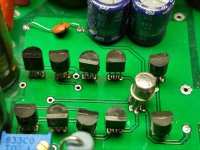
I have my first 4 Exicon casualties . Fortunately these MOSFETs were ordered as matched pairs meaning that the 18 N MOSFETs match between them , and the 18 P MOSFETs as well. So I still have some in the box. See the color dots on the package. I had beautiful fireworks inside home.
About the capacitors, compensations, etc. voltwide offered a suggestion, I think you guys are talking more or less the same thing here:
voltwide suggestion on post #33 see schematic
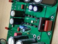
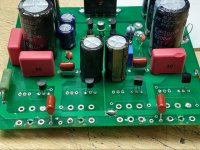
I will make all thees changes if you guys believe that the no MOSFETs board voltage test is OK and promising. For the voltage measurement test, there is no load at all. Just the originally installed Zobel with a 10n capacitor + 10 Ohm resistor. Somebody suggested 100nF for the cap. In this situation a tiny 50mV @100MHz signal can be seen in my Tek 2465. Even with power off I can see this strange oscillations, and believe me, I feel scared because I can't understand if this is normal, if it is an oscillation, an FM station nearby, ...... 😕😕😕 as I said my expertise is with my microprocessors and digital systems. I can help and give plenty of advice on that, in this case I only can sing Joe Cocker's "with a little help from my friends". Some pictures here of the making.
About the heat sinks, the ones I have here are not ideal and the available space in the board where all the transistors tightly coexist is very small. On top of this, with these transistors the only way is an epoxy shot, but once the heat sink is fixed it is hard to see and measure. So I decided to make the existing transistors sweat a little for the previous test and now I can fix the heat sink somehow. Also, I doubt that thermally connecting non heating transistors is a good idea. Up to know I detect that 4 of them need help, but some others are cool and near the ones that get hot. 😕
These 2 boards apparently are throwing the same voltages. Gate voltages seem to be more reasonable in the range of +/-0.9V to 1.1V, with the feedback trick done with 170 Ohms that I could get in my resistor box, as today I can't go get better values because of national holiday. Also R32 y R33 change their values or get open as I test and fail. I have replaced them a couple of times. This time I removed the SMDs and placed 2 matched 39 Ohms, sorry no 33 Ohms available today
So the situation is that the only good transistors for the job I have handy are 2N5551/2N5401. Replaced Q1 and Q5 for these high voltage devices and I am thinking to do the same with Q8 and Q2 if you guys agree, until I can get a Mouser order with the Zetex. Rick, unfortunately the PSW42(NPN)/-92(PNP) are non stocked at Mouser. If it would be my choice I would prefer MJE340/350 with a reasonable heat sink, but aparatusonitus says the Zetex are OK.
Of course Rick !
Another way to save output expenses -- only place one pair -- one N-ch, one P-ch. You can even just lift the Gate lead on the other two; well, don't leave it floating - tie it to the Source to make sure it stays off. And no-load, of course!
I have my first 4 Exicon casualties
. Fortunately these MOSFETs were ordered as matched pairs meaning that the 18 N MOSFETs match between them , and the 18 P MOSFETs as well. So I still have some in the box. See the color dots on the package. I had beautiful fireworks inside home.About the capacitors, compensations, etc. voltwide offered a suggestion, I think you guys are talking more or less the same thing here:
voltwide suggestion on post #33 see schematic
I will make all thees changes if you guys believe that the no MOSFETs board voltage test is OK and promising. For the voltage measurement test, there is no load at all. Just the originally installed Zobel with a 10n capacitor + 10 Ohm resistor. Somebody suggested 100nF for the cap. In this situation a tiny 50mV @100MHz signal can be seen in my Tek 2465. Even with power off I can see this strange oscillations, and believe me, I feel scared because I can't understand if this is normal, if it is an oscillation, an FM station nearby, ...... 😕😕😕 as I said my expertise is with my microprocessors and digital systems. I can help and give plenty of advice on that, in this case I only can sing Joe Cocker's "with a little help from my friends". Some pictures here of the making.
About the heat sinks, the ones I have here are not ideal and the available space in the board where all the transistors tightly coexist is very small. On top of this, with these transistors the only way is an epoxy shot, but once the heat sink is fixed it is hard to see and measure. So I decided to make the existing transistors sweat a little for the previous test and now I can fix the heat sink somehow. Also, I doubt that thermally connecting non heating transistors is a good idea. Up to know I detect that 4 of them need help, but some others are cool and near the ones that get hot. 😕
Attachments
-
 Mouser R27.jpg860.1 KB · Views: 288
 -
 R27 10K.jpg694.8 KB · Views: 234
 -
 IMG_20191118_161655889_HDR.jpg671.6 KB · Views: 221
 -
 IMG_20191118_163211582.jpg593.9 KB · Views: 232
 -
 Heat sink.jpg427.4 KB · Views: 221
 -
 Heat sink 2.jpg359.7 KB · Views: 90
 -
 Board without MOSFETs 2.jpg659.7 KB · Views: 102
 -
 Board without MOSFETs 1.jpg740.9 KB · Views: 123
Dear aparatusonitus:
Let's make the mods now that the boards seem to be more "normal". Please give me your opinion on the last measurements.
Let's agree that not everything can be done on these boards, not because it could take work, but just because is physically impossible. MJE340/MJE350 won't fit in the place designed for the tiny BC's or 2N5551/2N5401. Besides they a re BCE and not CBE. The leads are thicker. Just won't fit. I have lots of them here. So I will have to use the Zetex option ZTX758/658. I need one week for them to arrive, I will place the order today at Mouser. Don't know how I will manage to add heat sinks to all devices. The best solution is to redesign the whole board and I can't do that, I have 20 copied PCB's.
These Q7 and Q14 are in its place and are part of the original. If you prefer to eliminate them, that is very easy, they can be jumped over in the same PCB. Please tell me what is your best preference. This define R34 value at your choice. I would use all Zetex transistors.
I first tried to locate the coarse error in the boards. I found the error and corrected. Published voltages schematic. Now, with this corrected, we can go and make all of your suggestions, completely. As I said, we will have the Zetexes in 7 days, I hope that you will understand 🙂
Well...no room for heat sinks, so if you agree let's make it all with Zetex in 7 more days. Do you agree ?
Sure, but in this place of the board it is easy to install heat sinks, there is room enough. Please take a look te the pictures, you will probably agree.
Your opinion always welcome !
First let's clarify some things by referring to your last post/schematic:
Let's make the mods now that the boards seem to be more "normal". Please give me your opinion on the last measurements.
1) whether or not the amplifier uses Q7/Q14 pre-diver transistors. If the answer is yes, the current through them will need to be reduced by increasing the value of R34 to approx. 560-680 Ohms or go for Zetex transistors
Let's agree that not everything can be done on these boards, not because it could take work, but just because is physically impossible. MJE340/MJE350 won't fit in the place designed for the tiny BC's or 2N5551/2N5401. Besides they a re BCE and not CBE. The leads are thicker. Just won't fit. I have lots of them here. So I will have to use the Zetex option ZTX758/658. I need one week for them to arrive, I will place the order today at Mouser. Don't know how I will manage to add heat sinks to all devices. The best solution is to redesign the whole board and I can't do that, I have 20 copied PCB's.
These Q7 and Q14 are in its place and are part of the original. If you prefer to eliminate them, that is very easy, they can be jumped over in the same PCB. Please tell me what is your best preference. This define R34 value at your choice. I would use all Zetex transistors.
2) why the circuit still uses unnecessary C8/C17/C3/C4 compensation instead of a single capacitor (~15pF) from collector Q1 to gate J2
I first tried to locate the coarse error in the boards. I found the error and corrected. Published voltages schematic. Now, with this corrected, we can go and make all of your suggestions, completely. As I said, we will have the Zetexes in 7 days, I hope that you will understand 🙂
3) why the diagram still shows Q8=BC556B and Q2=BC546B when we concluded long ago that there should be at least 2N5401 and 2N5551 with heatsinks. In addition, Q2 and Q5 form a simple current mirror that must be designed with paired/match transistors of the same type.
Well...no room for heat sinks, so if you agree let's make it all with Zetex in 7 more days. Do you agree ?
4) Q3/Q4/Q6/Q13 driver transistors will need heatsinks anyway, whether they be Zetex or something else.
Sure, but in this place of the board it is easy to install heat sinks, there is room enough. Please take a look te the pictures, you will probably agree.
Your opinion always welcome !
Before we check off the rest of the suggestions list, there's something squirrel-y with the 2nd differential pair, Q10/Q11 -- any chance those naughty boys are flipped? I'm often wrong, but seem to remember that the BC546 series is one of those that is available in at least 2 different pinouts !!😉
Their Bases oughta be somewhere in the upper 22V range with the rails at 58.3V. And Q10's Emitter-Collector voltage looks suspiciously like 1 Vbe.
One other worrisome item: 54.4V on J2's Drain exceeds its rating. Maybe it was damaged when the Exicons blew off their faces.😱 In any event, nothing will balance (zero OP offset) after that until those Drains are within a couple hundred millivolts.
Also, agree with aparatusonitus about increasing R34; however, I like to get more work out of a driver stage myself (that's just me). Once the VAS has provided all the V-swing you need, succeeding stages ought to contribute a current gain of 10 at least. Consider 3k6 or 3k9 -- at least it'll be a little cooler when idling. (Then make sure it still sounds OK😉)
Cheers
Last edited:
Thank you Rick, I will check again. This why I wanted to be sure about the actual voltages.
Remember: these were a couple of working amplifier boards. One exploded. The other I have it intact and working. OK, OK, I know, very bad design. But this has been working for 10 years or more. I take this last working board as sample. It has MOSFETs installed.
So I made 20 copies of this original. The manufacturer is local and I not even had to draw the board. These are copies of the original Gerber file. No errors I think. All transistors and components were placed exactly to the original working board orientation. With the damaged board I could get the schematic. I had just one error, now corrected. Q7 and Q14 were missing. Pre drivers ...
I will check the voltages again, what you are pointing is interesting. Once I feel confident with the voltages of this ugly, perhaps badly designed circuit, I can continue with the proposed mods. Perhaps you read my last post, I need the Zetex transistors from Mouser.
But first we need to know if the voltages are acceptable or not. I could have made a mistake with the voltages transcription. I'll do it again so we can check, I still have an original without MOSFETs. ( the other channel).
Oh, gosh no -- I think this is a lovely design, IMHO.
In fact, everything we've talked about -- except maybe the compensation -- is what I would consider piddly stuff, or maybe 'old habits die hard'.
Glad you reminded me about the history -- I forget that way too often.
What seems to happen sometimes, with units that have long served well, even the 'exact replacement' p/n's are more modern devices, often with different performance over frequency. Then a compensation scheme that worked fine with 1990's devices falls a little short controlling the newer, usually faster, ones.
Another trick you can use to check the front end: Replace Q10/Q11 Base-Emitter junctions with 1N4148s - or whatever you have handy. Only bring the variac up to 15 or 20% of line. Then see that you're getting normal, well-balanced behavior from the input pair -- I'm still worried about J2. With the VAS staying off, the feedback path may wander; each touch with the x1 'scope probe will bring it back towards ground comfortably enough.
Oh, and, try not to worry about a few tens of millivolts oscillation a few seconds after cutting the power -- those big rail caps can supply all sorts of low-voltage frolic for many seconds.
Last edited:
Such a great advice and useful tips Rick.
This is what I feel ... you must also know that 20 original Hitachi 2SK1058/2SJ162 are on their way from Pacific Semiconductor in Canada. Great supplier. Will take a week or so. Just because my guess is that the new Exicons are slightly different (better, faster, lower Cin, etc) and this circuite loves the old ones.
When being so far from the big suppliers it takes time when testing and making changes. I have spend some money in 20 dual JFETs, PCB's, and lots of WIMA capacitors and SMD devices. But while I order the Zetex devices I will check this J2 issue and be back. Thank you guys for your patience.
What seems to happen sometimes, with units that have long served well, even the 'exact replacement' p/n's are more modern devices, often with different performance over frequency. Then a compensation scheme that worked fine with 1990's devices falls a little short controlling the newer, usually faster, ones.
This is what I feel ... you must also know that 20 original Hitachi 2SK1058/2SJ162 are on their way from Pacific Semiconductor in Canada. Great supplier. Will take a week or so. Just because my guess is that the new Exicons are slightly different (better, faster, lower Cin, etc) and this circuite loves the old ones.
When being so far from the big suppliers it takes time when testing and making changes. I have spend some money in 20 dual JFETs, PCB's, and lots of WIMA capacitors and SMD devices. But while I order the Zetex devices I will check this J2 issue and be back. Thank you guys for your patience.
Before we check off the rest of the suggestions list, there's something squirrel-y with the 2nd differential pair, Q10/Q11 -- any chance those naughty boys are flipped? I'm often wrong, but seem to remember that the BC546 series is one of those that is available in at least 2 different pinouts !!😉
Their Bases oughta be somewhere in the upper 22V range with the rails at 58.3V. And Q10's Emitter-Collector voltage looks suspiciously like 1 Vbe.
Agree, there is definitely something suspicious about Q11/Q8...obiwankenobi should check that they are the correct type (npn or pnp) as well as whether they are correctly oriented on pcb.
Correction, Q11's Emitter-Collector voltage looks suspiciously like 1 Vbe.
One other worrisome item: 54.4V on J2's Drain exceeds its rating. Maybe it was damaged when the Exicons blew off their faces.😱 In any event, nothing will balance (zero OP offset) after that until those Drains are within a couple hundred millivolts.
Agree, input j-fets could/should be damaged, fresh pair should be installed. Desoldering braid wire should be use for repair to prevent damage to pcb traces.
Dear aparatusonitus and Rick, all contents noted. Be sure that I am working on all this. Rather artesanal, it takes some time. Original Hitachi MOSFETs are on its way and also Zetex devices from Mouser. In the meantime I will replace and check orientation of every device in the VAS. Also 2N5656 dual JFET will be replaced with a fresh one. I am actually using this device that Mouser offers as a new direct replacement of the VISHAY original, the IFN5565 from InterFET.
Here is the datasheet of IFN5565
All possible suggested changes and deletions are to be done now. I'll be back to you guys, thank you.
Here is the datasheet of IFN5565
All possible suggested changes and deletions are to be done now. I'll be back to you guys, thank you.
aparatusonitus, thanks for fixing me on Q10/Q11 -- pro-o-obably shoulda quit typing while I was still awake ..
Granted, it is extra work but if it was me, I'd want to confirm proper loads on the JFETs before sticking in $23-worth of new part.
Hope your Holiday was good, OB1! -- and not too frustrating when there's no place open and you need to buy more Solder Wick.
Granted, it is extra work but if it was me, I'd want to confirm proper loads on the JFETs before sticking in $23-worth of new part.
Hope your Holiday was good, OB1! -- and not too frustrating when there's no place open and you need to buy more Solder Wick.
Last edited:
- Home
- Amplifiers
- Solid State
- Fixing and troubleshooting this MOSFET amplifier