@gannaji,
I'll attach the .asc file in the next post when I check a few things.
@Rick
In the given scheme, the right end of the C1 capacitor is attached to the VAS output node, so C1 sees the full output voltage and also bypasses Q2 at HF...according to an article by Samuel Groner C1 is a feedforward/compensation capacitor. The C15 is only there to balance the capacitive load seen by the drains of the input J-fets.
The reason I tried different compensation was that I was not happy with the simulated results for gain/phase margins...and that I was inclined to try new/unconventional solutions, which of course may not necessarily be good thing.😀
After sobering up (thanks Rick!), I went back to the previous simple solution with only one compensation capacitor, but with a high current in the differential tail (11mA total, 2 x 5.1mA for J-fetes + rest for biasing Q10/Q11cascade). It is worth noting that the lower end of the R35 is attached to the tail of the differential, thereby converting the cascade from fixed to floating allowing constant Vds over the input J-fetes.
It would also be a smart move to replace the R7 with a Vgs multiplier constructed around the lateral M-fet 2SK213-216 screwed on heatsink along with the output M-fets so we can easily bias the output stage and have a (more or less) constant output stage bias from completely cold to fully warmup amplifier.
Attachments
Yup. looks like I've got some study'in' to do -- thanks for the Samuel Groner reference, aparatusonitus. He writes well -- may take me a day or two to digest those 55 pages! And -- exactly what we're working on, is exactly what he described on page 39. Good stuff. Thanks again!
Cheers,
Rick
Cheers,
Rick
Welcome gannaji, enjoy, here we can learn with friends that have a lot of experience and good will.
Let me study the last info, I am sorry I was out for a job. I'll be back.
Thank you so much aparatusonitus and Rick
Let me study the last info, I am sorry I was out for a job. I'll be back.
Thank you so much aparatusonitus and Rick
Thank you aparatusonitus.
...and you still are paying attention to my questions and doubts. Please don't worry, family and your priorities are first, my friend. I can surely wait.
Anyway, here are some comments and questions that can be answered with no time pressure at all.
I will have to buy again from Mouser, because some values have changed and almost all the board uses SMDs 1206 components, in order to be precise with your new suggested schematic. Do you mind if I do ? It will take one more week (or a little less perhaps).
I have questions for you, if you please:
1. I have BC546B instead of BC547B, can they be used ?
2. no trimpot this time ? That would be fantastic. Please confirm.🙂
3. just 2 MOSFETs ? Simulation shows 110 W output @1kHz RMS, great ! Why original uses 4 devices ? Seems that 2 MOSFETs are OK, 21 W power dissipation each. 😕
4. could you specify power dissipation for R6, R7, R8 and R21 ?
5. what kind of caps should be use for C16, C17, C18 and C19 please ?
6. I have C2 and C14 220uF non polarized. Would they work ?
7. I have no room for R29 and R38. If they are mandatory I will try to place them but I would have to drill the PCB. Please specify type and PD please.
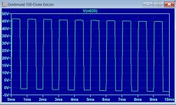
8. I am bad with LTSpice, just basic things. Why the output swings from almost 0V to 45V if I inject square wave @ 1kHz +750mV / -750mV p-p ?
9. which is the value of the quiescent bias current for the MOSFETs ?
Please see attached pictures. I am happy to learn.
Blessings for you all and families.
I apologize in advance for my slow reaction ... my family member's health requires full attention.
...and you still are paying attention to my questions and doubts. Please don't worry, family and your priorities are first, my friend. I can surely wait.
Anyway, here are some comments and questions that can be answered with no time pressure at all.
I will have to buy again from Mouser, because some values have changed and almost all the board uses SMDs 1206 components, in order to be precise with your new suggested schematic. Do you mind if I do ? It will take one more week (or a little less perhaps).
I have questions for you, if you please:
1. I have BC546B instead of BC547B, can they be used ?
2. no trimpot this time ? That would be fantastic. Please confirm.🙂
3. just 2 MOSFETs ? Simulation shows 110 W output @1kHz RMS, great ! Why original uses 4 devices ? Seems that 2 MOSFETs are OK, 21 W power dissipation each. 😕
4. could you specify power dissipation for R6, R7, R8 and R21 ?
5. what kind of caps should be use for C16, C17, C18 and C19 please ?
6. I have C2 and C14 220uF non polarized. Would they work ?
7. I have no room for R29 and R38. If they are mandatory I will try to place them but I would have to drill the PCB. Please specify type and PD please.
8. I am bad with LTSpice, just basic things. Why the output swings from almost 0V to 45V if I inject square wave @ 1kHz +750mV / -750mV p-p ?
9. which is the value of the quiescent bias current for the MOSFETs ?
Please see attached pictures. I am happy to learn.
Blessings for you all and families.
Attachments
I have questions for you, if you please:
1. I have BC546B instead of BC547B, can they be used ?
2. no trimpot this time ? That would be fantastic. Please confirm.🙂
3. just 2 MOSFETs ? Simulation shows 110 W output @1kHz RMS, great ! Why original uses 4 devices ? Seems that 2 MOSFETs are OK, 21 W power dissipation each. 😕
4. could you specify power dissipation for R6, R7, R8 and R21 ?
5. what kind of caps should be use for C16, C17, C18 and C19 please ?
6. I have C2 and C14 220uF non polarized. Would they work ?
7. I have no room for R29 and R38. If they are mandatory I will try to place them but I would have to drill the PCB. Please specify type and PD please.
8. I am bad with LTSpice, just basic things. Why the output swings from almost 0V to 45V if I inject square wave @ 1kHz +750mV / -750mV p-p ?
9. which is the value of the quiescent bias current for the MOSFETs?
1. Yes
2. Since worst case Vos is 10mV for 2N5565 x gain {10 mV x (1 + 7500/240)} = +/- 32,25mV max. ...I could live with that, but I'll see if trimmer can be put to null output DC offset.
3. Latest .asc file shows 2 pairs of m-fets per channel, dissipation is ~6W per each m-fet in when idling.
4. Just run DC op pnt in LTspice and hover you mouse pointer over component you want to check
5. Polystyrene/styroflex, silvered mica or MLCC/NP0 ceramic
6. They are so called feedback capacitor, ensures unity gain at DC. Also a low frequency pole (highpass roll-off) at fc = 1/{2 x Pi x R20 x (C2 + C14)/(C2 x C14)}. With C2 and C14 in schematic output DC offset is essentially 0V, with out +6,33mV. This will not be the case with real amplifier, see number 2.
7. R3/R37/R29/R38 are not needed if output m-fets are very closely match, beetwin same sex as well as opposite sex (N-ch to N-ch, P-ch to P-ch as well as N-ch to P-ch). It is very likely they are already match in your amp, so don't mix them. If that is not the case, use any 0.1-0.33R/5W resistor you can squeeze in.
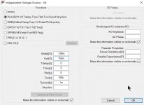
8. 'Cos LTspice will do anything to please you master obiwankenobi😉...use this PULSE(-.032 .032 0 {t_edge} {t_edge} {1/2/{freq}-t_edge} {1/{freq}}) instead for signal source V1. You will see square wave @ 20kHz +1V/-1V p-p. You can change freq. from 20kHz to anything with .param Freq=20k in upper right corner e.g. .param Freq=1k
9. With the R7 = 660 Ohm, quiescent current is ~100mA. You are advice to change R7 slighty to bias output m-fets to zero-tempco = 125mA, see transfer characteristic image Vgs vs Id in referent Exicon datasheet.
Thank you aparatusonitus, just to avoid spoiling your efforts, here are some points to remark before you bring new ideas and calculations.
If you are making the effort of considering offset null adjustment, please consider that the actual PCB's drawing has the trimpot connected to Q10 and Q11 collectors instead of J1 and J2 sources. The original amp designer copied the same system that Goldmund used in Mimesis 3 and 9. But if you placed the trimpot over J1 and J2 you may probably have a good reason. Placing the trimpot south instead of north is almost imposible because the board has a ground plane in that area and no enough room. It should then be fixed somewhere else or cut traces and run cables of no less than 1.5" or 5 cm. I don't know how harmful could this cabling be...you tell me please.😉
Understood...my question is if the non polarized 220 uF caps I have plenty may be used in parallel instead of your series polarized 1000uF (1mF) ?😕
I bought 36 Exicon MOSFETs, 18 Nch and 18 Pch and paid a little more because the distributor in GB, Profusion Ltd, offers 'S' suffix parts that are perfectly paired (same sex), and have a same color dot for each same type paired devices. So if you agree, I will not use these R's. What happens if the MOSFETs are not paired ? This would happen if I use the original Hitachi's I found in Canada and that are in the mail right now. Using this additional R technique could make it possible for these unpaired MOSFETs to be used ?
I'll try this, but please, some other time, explain me how come it does not work with a single square wave generated as a pulse. I am very curious about this.🙄
Finally...
Considering this last schematic version, do you think that I can buy the new part values from Mouser now ?
Thank you so much aparatusonitus, hope your parents be OK soon !
2. Since worst case Vos is 10mV for 2N5565 x gain {10 mV x (1 + 7500/240)} = +/- 32,25mV max. ...I could live with that, but I'll see if trimmer can be put to null output DC offset.
If you are making the effort of considering offset null adjustment, please consider that the actual PCB's drawing has the trimpot connected to Q10 and Q11 collectors instead of J1 and J2 sources. The original amp designer copied the same system that Goldmund used in Mimesis 3 and 9. But if you placed the trimpot over J1 and J2 you may probably have a good reason. Placing the trimpot south instead of north is almost imposible because the board has a ground plane in that area and no enough room. It should then be fixed somewhere else or cut traces and run cables of no less than 1.5" or 5 cm. I don't know how harmful could this cabling be...you tell me please.😉
6. They are so called feedback capacitor, ensures unity gain at DC. Also a low frequency pole (highpass roll-off) at fc = 1/{2 x Pi x R20 x (C2 + C14)/(C2 x C14)}. With C2 and C14 in schematic output DC offset is essentially 0V, with out +6,33mV. This will not be the case with real amplifier, see number 2.
Understood...my question is if the non polarized 220 uF caps I have plenty may be used in parallel instead of your series polarized 1000uF (1mF) ?😕
7. R3/R37/R29/R38 are not needed if output m-fets are very closely match, beetwin same sex as well as opposite sex (N-ch to N-ch, P-ch to P-ch as well as N-ch to P-ch). It is very likely they are already match in your amp, so don't mix them. If that is not the case, use any 0.1-0.33R/5W resistor you can squeeze in.
I bought 36 Exicon MOSFETs, 18 Nch and 18 Pch and paid a little more because the distributor in GB, Profusion Ltd, offers 'S' suffix parts that are perfectly paired (same sex), and have a same color dot for each same type paired devices. So if you agree, I will not use these R's. What happens if the MOSFETs are not paired ? This would happen if I use the original Hitachi's I found in Canada and that are in the mail right now. Using this additional R technique could make it possible for these unpaired MOSFETs to be used ?
8. 'Cos LTspice will do anything to please you master obiwankenobi...use this PULSE(-.032 .032 0 {t_edge} {t_edge} {1/2/{freq}-t_edge} {1/{freq}}) instead for signal source V1. You will see square wave @ 20kHz +1V/-1V p-p. You can change freq. from 20kHz to anything with .param Freq=20k in upper right corner e.g. .param
Freq=1k
I'll try this, but please, some other time, explain me how come it does not work with a single square wave generated as a pulse. I am very curious about this.🙄
Finally...
Considering this last schematic version, do you think that I can buy the new part values from Mouser now ?
Thank you so much aparatusonitus, hope your parents be OK soon !
I can't remember -- do we have a decent-quality LTSpice model for the Hitachi outputs?
If so, that would go a long way toward answering some of the questions we (or .. maybe it's just me😕) still have about current-sharing and stability -- for those OP's, anyway.
If you had to, the output Source resistors could be fitted standing upright next to the OP, with its lower leg in an 'S' shape and soldered into the original Source lead hole. Then the Source lead bent into a 'U' shape (not going into its original mounting hole), it could connect 'dead bug style' to the upper lead of the resistor. This probably wouldn't work at all for a fast MOSfet in a switching application, but I think it'll be OK here. At least it would save drilling additional holes. Then if those resistors turn out not to be necessary, we haven't buggered it up to remove them!😉
Well-wishes and good-health-hopes for the aparatusonitus family.
Regards,
Rick
PS -- Oh, and for initial testing, the 220uF non-polars are fine -- even just one. Slight sub-20Hz rolloff is the only loss.
PPS -- If it was me, I wouldn't order more parts 'til the Hitachi's have been tested .. but that's me.
Last edited:
OK, dunno yet whether its any good or not, but found this:
FROM: electronics cad, Spice model 2SK1058 2SJ162
*N-Channel 160V 7A
.MODEL 2SK1058 NMOS (VTO=-767.135M KP=20U L=2U W=20.8177M GAMMA=0 PHI=600M
+ LAMBDA=862.511U CBD=915.478P IS=10F CGSO=1.65276N CGDO=1.65276N TOX=0 NSUB=0
+ TPG=1 UO=600 RG=10 RDS=1MEG GDSNOI=0)
*
*P-Channel -160V -7A
.MODEL 2SJ162 PMOS (VTO=842.191M KP=20U L=2U W=21.3317M GAMMA=0 PHI=600M
+ LAMBDA=20.7068M RD=837.194M CBD=1.32272N IS=10F CGSO=1.65276N CGDO=1.65276N
+ TOX=0 NSUB=0 TPG=1 UO=600 RG=10 RDS=1MEG GDSNOI=0)
*
Hey Rick ! Always nice to hear from you. Your posts are very interesting, it's me that don't match your knowledge level. I'm trying though ...😛
Maybe you will find the attached models interesting. They worked for me. However, you will have to chose for the best from the different files.
I'll try to do this, but Rick my Exicon MOSFETs are paired from factory. Do you believe these Rs are still necessary? Why ?

The board accommodates 2 in parallel in an identical circuit. I'll try this first.
Actually I started 2 lines of investigation. I will assemble 2 boards, one with the original working schematic but with the original Hitachi MFs. They are now in customs, I must wait a little. The other line is following aparatusonitus schematic. In the first case I need to know why it is so hard to make this amp work as a replica with Exicon MFs. In the second one I think that we have the opportunity to make this nice interesting option work ! If it does, gentlemen, you can count with the Gerber files of a new PCB, this time done with my own style and fixing so many uncomfortable issues. For aparatusonitus fixes I will need to order more parts from Mouser because some part values are different, and specially because the original PCB was designed around SMT, eg: 33 Ohms, 400V 5% 1206 Rs are not available locally in small QTY's, just 5000 pcs rolls, by special order. Evey order takes around $150 + $35 freight and then 50% customs duty 😀 that you pay cash when DHL or FedEx delivers at my door.
I can't remember -- do we have a decent-quality LTSpice model for the Hitachi outputs?
Maybe you will find the attached models interesting. They worked for me. However, you will have to chose for the best from the different files.
If you had to, the output Source resistors could be fitted standing upright next to the OP, with its lower leg in an 'S' shape and soldered into the original Source lead hole...
I'll try to do this, but Rick my Exicon MOSFETs are paired from factory. Do you believe these Rs are still necessary? Why ?
ha haaa ! Yeah !'dead bug style'
PS -- Oh, and for initial testing, the 220uF non-polars are fine -- even just one. Slight sub-20Hz rolloff is the only loss.
The board accommodates 2 in parallel in an identical circuit. I'll try this first.
PPS -- If it was me, I wouldn't order more parts 'til the Hitachi's have been tested .. but that's me.
Actually I started 2 lines of investigation. I will assemble 2 boards, one with the original working schematic but with the original Hitachi MFs. They are now in customs, I must wait a little. The other line is following aparatusonitus schematic. In the first case I need to know why it is so hard to make this amp work as a replica with Exicon MFs. In the second one I think that we have the opportunity to make this nice interesting option work ! If it does, gentlemen, you can count with the Gerber files of a new PCB, this time done with my own style and fixing so many uncomfortable issues. For aparatusonitus fixes I will need to order more parts from Mouser because some part values are different, and specially because the original PCB was designed around SMT, eg: 33 Ohms, 400V 5% 1206 Rs are not available locally in small QTY's, just 5000 pcs rolls, by special order. Evey order takes around $150 + $35 freight and then 50% customs duty 😀 that you pay cash when DHL or FedEx delivers at my door.
Attachments
If you are making the effort of considering offset null adjustment, please consider that the actual PCB's drawing has the trimpot connected to Q10 and Q11 collectors instead of J1 and J2 sources. The original amp designer copied the same system that Goldmund used in Mimesis 3 and 9. But if you placed the trimpot over J1 and J2 you may probably have a good reason. Placing the trimpot south instead of north is almost imposible because the board has a ground plane in that area and no enough room. It should then be fixed somewhere else or cut traces and run cables of no less than 1.5" or 5 cm. I don't know how harmful could this cabling be...you tell me please.😉
I'll have to work something out and place dc offset trimer where is use to be - north. Running few mA thru trimmer wiper is the thing that warries me.
Btw, you can always put small extra board (vertically or horizontally) if modification is needed.
Understood...my question is if the non polarized 220 uF caps I have plenty may be used in parallel instead of your series polarized 1000uF (1mF) ?😕
You can put non-polarized caps in parallel if you wish.
I bought 36 Exicon MOSFETs, 18 Nch and 18 Pch and paid a little more because the distributor in GB, Profusion Ltd, offers 'S' suffix parts that are perfectly paired (same sex), and have a same color dot for each same type paired devices. So if you agree, I will not use these R's. What happens if the MOSFETs are not paired ? This would happen if I use the original Hitachi's I found in Canada and that are in the mail right now. Using this additional R technique could make it possible for these unpaired MOSFETs to be used?
If the m-fets are not match and without source resistors there will always be one in the group that will do most of the work...source resistances serve to equalize m-fet work with local feedback.
Considering this last schematic version, do you think that I can buy the new part values from Mouser now ?
Not yet...I would like to see some more opinions/options from others.
aparatusonitus
🙂
OK ! Let's wait a little then...Not yet...I would like to see some more opinions/options from others.
🙂
Surprised it lasted as long as it did with Q1,Q5 rated at 80v exposed to 120v when driven hard. KSC3503,KSA1381 should be here. increasing the gate resistor a few hundred ohms should end the oscillation. 2N5551, 2N5401 won't run any cooler but can take the voltage.
Hello stocktrader200 you are very welcome, greetings from Buenos Aires, Argentina.
Me too. I worked perfectly 10+ years with great sound. One day we had fireworks.Surprised it lasted as long as it did with Q1,Q5 rated at 80v exposed to 120v when driven hard
I tried everything,75, 100, 150, 300 and 680 Ohms. It is an FM station.increasing the gate resistor a few hundred ohms should end the oscillation
Yes! Good idea. Just because they have a hole for the heat sink. Half of the devices needs them. My next amp will use similar Onsemi MJE340/350. I ordered 200 pcs ZTX658/758 THAT aparatusonitus suggested given the conditions of the actual PCB. KSC3503,KSA1381 won't fit in. Sorry, you may probably like to read the story and the pictures of the problem, etc. I am not making a new PCB by now, I have to use the ones I have (around 18 pcs). The reasons for this I explained before...The only change was Exicon MOSFETs by original Hitachi...KSC3503,KSA1381 should be here
Yes, correct, but I am now testing the Zetex / Diodes, Inc devices + some kind of het sinking if placed from the bottom side where there is enough room. A bad design to my knowledge. Great friends are brainstorming with me to see if we can make it work again.2N5551, 2N5401 won't run any cooler but can take the voltage.
Yes, correct, but I am now testing the Zetex / Diodes, Inc devices + some kind of het sinking if placed from the bottom side where there is enough room. A bad design to my knowledge. Great friends are brainstorming with me to see if we can make it work again.
With current schematic you won't need any heatsink for any TO92/E-line small signal transistors, all are within SOA so there is no need to put any on the bottom side of the pcb either. They will ran hot, but they can take it in the long run...Since they are group in two strait line on the pcb, small heatsink enclosing all or each group would make their life easier.
Ohh ! Great aparatusonitus !
Regular small clip heat sinks for TO-92 (regular package) won't fit new modified TO-92-3 small case of the Zetex family. I would like to use some means of heat sinking, I'll find the way
You know ... I suspect that the high temperature of the BC5xx used in the original board may have caused that the solder melted or at least maintained near almost near liquid state that in many years produced some kind of oxide that made some device not to establish good electric contact with the rest of the circuit and ...bang !
What happens if I just thermally connect Q1, Q2, Q5 and Q8 ?
Regular small clip heat sinks for TO-92 (regular package) won't fit new modified TO-92-3 small case of the Zetex family. I would like to use some means of heat sinking, I'll find the way
You know ... I suspect that the high temperature of the BC5xx used in the original board may have caused that the solder melted or at least maintained near almost near liquid state that in many years produced some kind of oxide that made some device not to establish good electric contact with the rest of the circuit and ...bang !
Since they are group in two strait line on the pcb, small heatsink enclosing all or each group would make their life easier.
What happens if I just thermally connect Q1, Q2, Q5 and Q8 ?
Thank you aparatusonitus , yes, I understand. Although the transistors are placed in single lines, it is difficult to thermally isolate each pair. I'll start for the hottest ones.
Those Exicons should work just fine, even without the 0.1R's on the Sources (sorry aparatusonitis), but I'm open to discussion. MOSFETs have the opposite curve from BJT's over temp: Increasing temp causes decreasing conduction. They tend to share inherently.
But R7 will probably need to change -- maybe put in a temporary trimpot, 2k or 5k in parallel with 1k2 or 1k5. (The parallel fixed resistor being to limit maximum conduction for those inevitable scratchy spots in the trimpot.) Once a suitable value is determined, a single metal film part will suffice.
And the balance between Nch and Pch probably deserves investigating, if we are to believe the published curves at least. The threshold for 100mA conduction for the Nch is Vgs=0.54, while the Pch is 1.10V. (The graph doesn't specify Vds.) While the earlier stages will correct the output offset, it would probably be at the expense of linearity or unipolar headroom.
Sorry for the delay .. Yesterday at about this time, I was typing away on a bigger bucket of words, when a combination of pilot error and beer sent those hard-wrought notions to bit heaven! 😡
Cheers,
Rick
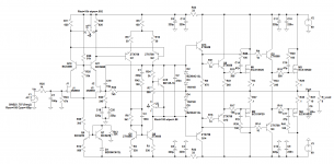
Well, I think I've reached the limit in the context of the default boundaries...I can't do better than the attached schematic, so here I draw the line. Now, I leave the development of the schematic with possibly better, more elegant solutions to others.🙂
Changes from the previous schematic:
- added trimmer U1 for output DC offset control, if wiper goes open, output stage bias will increase ~13%
-added Vbe multiplier built around Q15 and associated components (trimmer U2, R34, R7, C2), if wiper goes open, output stage bias will be few mA. With a given spice model of bjt's, m-fets, and resistors values around Q15, amp is slightly temperature overcompensated. The correct values will need to be determined experimentally on real McCoy.
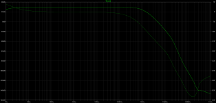
- Zobel network (C1 + R42) added to Q1/Q2 collectors, network is part of compensation as well as serve as frequency/phase curve smoothing. Not in the most favorable location (on the left is a relatively low impedance output from the current mirror while on the right is a high impedance output from VAS. It would be preferable to put it on the collectors Q10/Q11 (or the bases Q1/Q2), where the impedances at both ends are in balance, but in the simulator this did not turn out to be a good solution...the stability as well as the response to the capacitive load of the output seemed worse.
- Zobel added over all M-fetes...you know...belt and suspenders approach.
Well, that's all from me...(for now)😉
Changes from the previous schematic:
- added trimmer U1 for output DC offset control, if wiper goes open, output stage bias will increase ~13%
-added Vbe multiplier built around Q15 and associated components (trimmer U2, R34, R7, C2), if wiper goes open, output stage bias will be few mA. With a given spice model of bjt's, m-fets, and resistors values around Q15, amp is slightly temperature overcompensated. The correct values will need to be determined experimentally on real McCoy.
- Zobel network (C1 + R42) added to Q1/Q2 collectors, network is part of compensation as well as serve as frequency/phase curve smoothing. Not in the most favorable location (on the left is a relatively low impedance output from the current mirror while on the right is a high impedance output from VAS. It would be preferable to put it on the collectors Q10/Q11 (or the bases Q1/Q2), where the impedances at both ends are in balance, but in the simulator this did not turn out to be a good solution...the stability as well as the response to the capacitive load of the output seemed worse.
- Zobel added over all M-fetes...you know...belt and suspenders approach.
Well, that's all from me...(for now)😉
Attachments
-
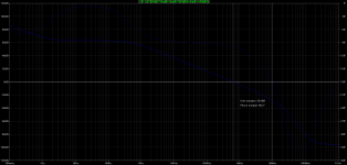 Goldmund 330 Clone Exicon phase and gain margines.png15 KB · Views: 172
 -
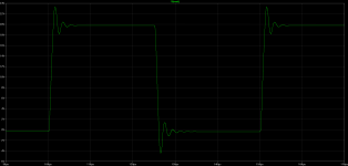 Goldmund 330 Clone Exicon overshoot 1u+8R.png9.6 KB · Views: 163
 -
 Goldmund 330 Clone Exicon clipping.png12.3 KB · Views: 158
 -
 Goldmund 330 Clone Exicon bode.png13.4 KB · Views: 187
 -
 Goldmund 330 Clone Exicon sch.png60.2 KB · Views: 206
 -
Goldmund 330 Clone Exicon.asc17.1 KB · Views: 87
-
 Goldmund 330 Clone Exicon tempco.png9.8 KB · Views: 113
Thank you Rick and aparatusonitus (Ivo if you allow me , I am Robert or Bob myself if you prefer 🙂), please excuse me, I m returning from a short trip out of town. Tonight I'll be back for some comments and questions. Rick about unpaired MOSFETs, this is really a good point for conversation and learning in my case, related to the 0.1 Ohms source resistors. The scratchy pots always worries me. Your solution is very interesting !

All contents read but I'll ask in detail later. aparatusonitus thank you for such an interesting contribution. Of course this version needs a fresh new PCB that I could design with your supervision, guys. First I will put my energy in fixing the original amp. I also agree that Exicon MFs must work fine. As soon as I can finish making the changes on the originals, we could devote ourselves to the new aparatusonitus version with a new PCB. Gerber files for you 2 friends are granted.
FYI, Buenos Aires is 3 hours ahead of Kansas City and 4 hours before Split (Spalato) or Zagreb
See you later ! Thank you !
Haaaa ha ha!Yesterday at about this time, I was typing away on a bigger bucket of words, when a combination of pilot error and beer sent those hard-wrought notions to bit heaven!
All contents read but I'll ask in detail later. aparatusonitus thank you for such an interesting contribution. Of course this version needs a fresh new PCB that I could design with your supervision, guys. First I will put my energy in fixing the original amp. I also agree that Exicon MFs must work fine. As soon as I can finish making the changes on the originals, we could devote ourselves to the new aparatusonitus version with a new PCB. Gerber files for you 2 friends are granted.
FYI, Buenos Aires is 3 hours ahead of Kansas City and 4 hours before Split (Spalato) or Zagreb
See you later ! Thank you !
- Home
- Amplifiers
- Solid State
- Fixing and troubleshooting this MOSFET amplifier