Hello friends ! Yes, a long holiday monday included.
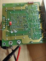
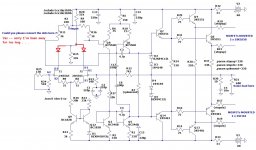
Please find the measurements of the only original amplifier working board.
Remember that this is the original board, no mods, with design errors, but working. The only dramatic difference Q8 collector, now 15.1V instead of -45.9V of the faulty copied version 😱😱😱
Tested at no load, input shorted to ground, as Rick said , some measured points near de dual JFET, the moment they were touched by the voltmeter tip showed strong oscillation that ceased immediately when the measurement ended. Very stable behaviour, no MOSFETs bias current with actual R7 = 330 Ohm. Output showed 0mV DC. really don't understand how this can sound so good without quiescent current.
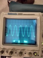
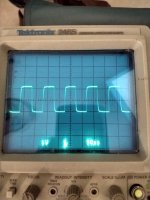
After this test, I connected a small 8 Ohms speaker and applied sine and square signal from 1 to 100 kHz, showing to work perfectly well. Heat in some of the VAS transistors? Of course YES ! A lot of heat.
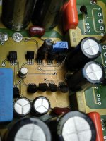
As we wait for the Mouser parts and Hitachi original MOSFETs coming from Canada, I thought that this could show some interesting details. I am now realizing that I bought 20 Hitachi MOSFEts that will be hardly paired, so the Exicons win.
I think that in the copied version of the boards, with the mods done, I will place the Zetex transistors on the bottom side of the board so to arrange some possible heat sinking. I have lots of room in the cabinet to do this.
Please find the measurements of the only original amplifier working board.
Remember that this is the original board, no mods, with design errors, but working. The only dramatic difference Q8 collector, now 15.1V instead of -45.9V of the faulty copied version 😱😱😱
Tested at no load, input shorted to ground, as Rick said , some measured points near de dual JFET, the moment they were touched by the voltmeter tip showed strong oscillation that ceased immediately when the measurement ended. Very stable behaviour, no MOSFETs bias current with actual R7 = 330 Ohm. Output showed 0mV DC. really don't understand how this can sound so good without quiescent current.
After this test, I connected a small 8 Ohms speaker and applied sine and square signal from 1 to 100 kHz, showing to work perfectly well. Heat in some of the VAS transistors? Of course YES ! A lot of heat.
As we wait for the Mouser parts and Hitachi original MOSFETs coming from Canada, I thought that this could show some interesting details. I am now realizing that I bought 20 Hitachi MOSFEts that will be hardly paired, so the Exicons win.
I think that in the copied version of the boards, with the mods done, I will place the Zetex transistors on the bottom side of the board so to arrange some possible heat sinking. I have lots of room in the cabinet to do this.
Attachments
-
 IMG_20191119_204738476_HDR.jpg613.5 KB · Views: 284
 -
 IMG_20191119_204844120_HDR.jpg438.3 KB · Views: 257
 -
 IMG_20191119_204850313_HDR.jpg558.2 KB · Views: 261
 -
 IMG_20191119_204902975_HDR.jpg521.5 KB · Views: 251
 -
 IMG_20191119_204609107_HDR.jpg476.4 KB · Views: 251
 -
 IMG_20191119_204629182_HDR.jpg470.8 KB · Views: 143
 -
 Captura_001358.jpg479.9 KB · Views: 182
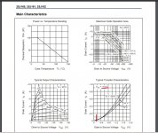
Those certainly are much nicer voltages. Could there be a '-' sign missing on Q14, Q13, Q3, and Q5's Collector measurements? If so everything makes sense.
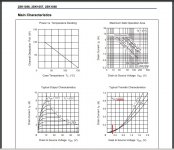
If the Renesas data sheets for the 2SK1058 and 2SJ162 are representative, these MOSFET's are rather low threshold - they start conducting almost as soon as Vgs moves from zero. At the 0.23 and -0.16 measured, looks like a decent quiescent flow -- maybe 40 - 50 mA, maybe 80 - 120, depending on how much more encouragement the 5-times-higher Drain voltage (than the 10V on the graph) gives. In any case, something is dropping the main rails by 0.8V from the values measured with outputs removed. And those sure are plenty pretty 10 kHz 'scope traces.
This is coming along nicely.
Good on ya'
Attachments
Interesting data dear Rick, in the afternoon today I will recheck the values again for this working board. If you suspect these negative signs I will do it again. You will notice a green large 0.1 Ohm 3W 1% resistor standing near the Hitachi MOSFETs. I cut the trace and placed it there to check the quiescent current of the MOSFETs with no signal, input grounded and it shows 0mA ! YES ! No current. Now I think that these guys couldn't inject more current there because of excessive heating.
I built a similar clone a couple of years ago and I could make 130 mA flow through each 4 devices Semelab BUZ900/BUZ905. Studying these Hitachi datasheets you brought I guess how different and compatible are the Hitachis, the Semelabs and the Exicons for these output stages ? Are they real replaceable without adjusting circuit values ?
Also, how delicate is soldering the dual JFET in its place. Because of my 65 years old I remember to do so with the soldering iron unplugged from mains as an old advice since I was almost a child and used some JFET in my HAM radio experiments. Your opinion is important here, because I could be harming them without knowing. I also recall that some devices came from factory with a small metal ring that shorted the leads between them while manipulating and soldering. Now these devices come without any protection from Mouser, just the plastic (non antistatic) bag.
You may like to read this Texas Instruments App note that compares output MOSFETs , quiescent currents, distortions and power, as you are an acute observer. Hope you all guys find it useful.
Attachments
I never in my life applied these electrostatic precautions when soldering any FETs and other stuff. And the pn-junction of a JFET is nothing but a reverse biased Si-Diode. If you do not pull your woolen pullover immediately before touching the pins there is no real danger.
Wool is safe from static, synthetic fibres are the problem. If you live in a damp climate and wear cotton and wool without nylon carpets you usually don't see much static and can be lucky (except during very cold winter weather when the air is much drier indoors).
Removing a synthetic fleece top can reliably wake up my computer from sleep from > 1 metre away!
If there is static around then any MOSFET can be destroyed instantly by improper handling without even realizing it (sometimes it will appear degraded, not fully broken).
Removing a synthetic fleece top can reliably wake up my computer from sleep from > 1 metre away!
If there is static around then any MOSFET can be destroyed instantly by improper handling without even realizing it (sometimes it will appear degraded, not fully broken).
Mark ...
That's real remote control 😱. Here in Buenos Aires we can sometimes have some static in rare dry days, but the mean %RH is around >70% all the year, so it is very unlikely for components to be exposed. Yes, we take care with too much air conditioning, certain kind of clothing and carpets.
Removing a synthetic fleece top can reliably wake up my computer from sleep from > 1 metre away!
That's real remote control 😱. Here in Buenos Aires we can sometimes have some static in rare dry days, but the mean %RH is around >70% all the year, so it is very unlikely for components to be exposed. Yes, we take care with too much air conditioning, certain kind of clothing and carpets.
MOSFET's are surely much less rugged than ordinary junctions. We don't have the luxury of 70%RH here (bet your electrons are much friendlier as a result), but ordinary precautions are all that I've are ever needed.
- don't set the part on the bench while it waits
- reach in to the anti-static bag to free it, rather than pucker the bag and dump it out
- grab the chassis or a ground trace as you fit the part
But that's for a MOSFET, which, even though your IRF5565 isn't, it IS a $23 part. Seems like the small bit of extra effort/trouble would not be entirely wasted -- even if unnecessary.
I do think it worthwhile -- maybe while you're waiting for the Zetex's -- to put a pair of diodes (almost anything would suffice) in place of the B-E junctions of Q10 and Q11. By checking the health of the original JFet, you may find it working well enough to complete and test the many other changes. That would allow saving the new, $23, six-legged part 'til every other issue has been resolved .. but that's just me.
Only once, in my early trials with CMOS, was a failure most likely due to static. But hey -- we're a similar vintage - I'm 63 -- you probably had fun with some 4000-series parts once upon a time, too, eh?😉
Oh, and thanks for that TI App Note you linked.
Last edited:
Rick, sometime I delay a little in paying attention to some issues, please excuse me, but ...
I understand what you say about preserving $23 on the 2N5565 devices, but could you please connect the dots and show me how the 1N4148s would be placed in the circuit instead of Q10 and Q11 ? What you are trying to say is that testing with diodes junctions we could know if the dual JFET is healthy or not. But, I'm sorry, please write your idea down over one of the schematics here. I don't get it exactly ...
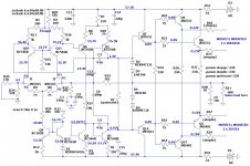
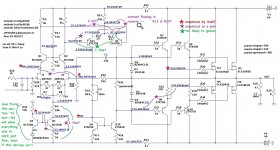
The other schematic is the last check of all the voltages in the circuit of this working original amp, as promised. This is a dangerous operation because the transistor's leads are so close between them that it requires concentration and somebody helping to take notes. My voltmeter, being a very noble instrument, clearly introduces some capacitance and/or noise that triggers the device to oscillate. There are question marks in those troublesome points. Just by touching there the amp switches to a strong oscillation that made the MOSFETs hot, I had to cut power. Nothing happened, it still works fine, but the readings may be very inaccurate in just those points, being the amp and oscillator at that moment. How can I measure there without disturbing the circuit ? 😕
BTW, the Zetex are now flying over Brasil, Mouser+DHL made it really fast. I think that I will have the box on monday over my desk 😀
Here are some papers ...
I do think it worthwhile -- maybe while you're waiting for the Zetex's -- to put a pair of diodes (almost anything would suffice) in place of the B-E junctions of Q10 and Q11. By checking the health of the original JFet, you may find it working well enough to complete and test the many other changes. That would allow saving the new, $23, six-legged part 'til every other issue has been resolved .. but that's just me.
I understand what you say about preserving $23 on the 2N5565 devices, but could you please connect the dots and show me how the 1N4148s would be placed in the circuit instead of Q10 and Q11 ? What you are trying to say is that testing with diodes junctions we could know if the dual JFET is healthy or not. But, I'm sorry, please write your idea down over one of the schematics here. I don't get it exactly ...
The other schematic is the last check of all the voltages in the circuit of this working original amp, as promised. This is a dangerous operation
because the transistor's leads are so close between them that it requires concentration and somebody helping to take notes. My voltmeter, being a very noble instrument, clearly introduces some capacitance and/or noise that triggers the device to oscillate. There are question marks in those troublesome points. Just by touching there the amp switches to a strong oscillation that made the MOSFETs hot, I had to cut power. Nothing happened, it still works fine, but the readings may be very inaccurate in just those points, being the amp and oscillator at that moment. How can I measure there without disturbing the circuit ? 😕BTW, the Zetex are now flying over Brasil, Mouser+DHL made it really fast. I think that I will have the box on monday over my desk 😀
Here are some papers ...
Attachments
Zetex transistors arrived. I will work on the board to make replacements and mods. I will report as I have results.
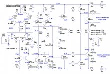
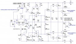
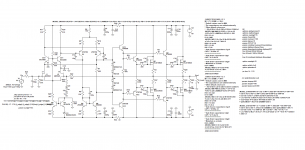
OK, I am working on a new, fresh PCB. Unfortunately the PCBs won't withstand further soldering and desoldering of components. So all fresh components. In the meantime, here is the simulation of the modifications proposed by aparatusonitus.
I hope that you are still there guys, and hope you'll understand that buying parts being so far takes time. Sorry for that. But I now have a lot of good Zetex transistors for testing. I will have to place them on the bottom side of the PCB, so I could probably fix some heat sinking. There is plenty of room there.
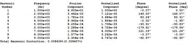
The files I am sharing with you contain the simulation results, schematic, full output power waveform, THD, frequency and phase response, static voltages with grounded input and a compressed file with the LTspice .asc file + a couple of needed models.
Quiescent current for each MOSFET adjusted for 127 mA, dc offset = 0.2V
Transistor's power dissipation is as follows:
Q9 Q7 Q10 Q8 / 253 mW
Q11 Q5 / 393 mW
Q6 / 5 mW
Q12 / 384 mW
Q4 / 1 mW
Q3 / 27 mW
Q1 & Q2 / 35 mW
J1 & J2 22 mW each device
M3 M4 M5 M6 7.6 W quiescent // 21 W full output power each device
Output power shows 72 W RMS (I think should be some more )
The pre driver transistors shown in previous versions as Q7 and Q14 are not present in aparatusonitus proposed mod. I can easily bypass them in the PCB.
For the test I will use just 2 MOSFETs as rick suggested.
Any suggestion is very welcome, before final test.
Thank you !
I hope that you are still there guys, and hope you'll understand that buying parts being so far takes time. Sorry for that. But I now have a lot of good Zetex transistors for testing. I will have to place them on the bottom side of the PCB, so I could probably fix some heat sinking. There is plenty of room there.
The files I am sharing with you contain the simulation results, schematic, full output power waveform, THD, frequency and phase response, static voltages with grounded input and a compressed file with the LTspice .asc file + a couple of needed models.
Quiescent current for each MOSFET adjusted for 127 mA, dc offset = 0.2V
Transistor's power dissipation is as follows:
Q9 Q7 Q10 Q8 / 253 mW
Q11 Q5 / 393 mW
Q6 / 5 mW
Q12 / 384 mW
Q4 / 1 mW
Q3 / 27 mW
Q1 & Q2 / 35 mW
J1 & J2 22 mW each device
M3 M4 M5 M6 7.6 W quiescent // 21 W full output power each device
Output power shows 72 W RMS (I think should be some more )
The pre driver transistors shown in previous versions as Q7 and Q14 are not present in aparatusonitus proposed mod. I can easily bypass them in the PCB.
For the test I will use just 2 MOSFETs as rick suggested.
Any suggestion is very welcome, before final test.
Thank you !
Attachments
I would not go for dc-coupling. It is irrelevant to sound and brings problems like high DC-offset - like your 0,2V.
Furthermore I do not see any advantage in using the expensive double JFET - 2BJTs out of the box will do as well.
Furthermore I do not see any advantage in using the expensive double JFET - 2BJTs out of the box will do as well.
Thank you voltwide, as I explained before in many pictures and posts, I can't make those changes in this board. This has worked with a dual JFET 10+ years. I am trying to reconstruct blown amplifiers. Changes and mods can be done but everything must be possible in the 20 PCB's that are a replica of the working originals. I am open to materially possible changes.
What I need now is advice with the new schematic suggested. I will wait a little for replies of the friends that were helping me. Silence by now.
What I need now is advice with the new schematic suggested. I will wait a little for replies of the friends that were helping me. Silence by now.
I will wait a little for replies of the friends that were helping me. Silence by now.
You are NOT alone, I'm working on new schematic, but your posts give me some doubts.
If I understand correctly, any modification must be:
- easily incorporated into existing pcb (you have a plenty)
- the "designer" is free to choose single EF + SF or double EF + SF for output stage (EF = emitter follower; SF = source follower)
Right?
Thank you so much aparatusonitus ! No doubts this side !
The problem is this:
My first schematics try to show exactly what my PCB does.
The designer (not me !!) made some terrible mistakes such as very small pads and very close pads, no space in between. This makes very difficult servicing and parts replacement without damaging the PCB. Believe me !
Now, your new proposed design , eliminated my last correction in which I included the missing Q7 and Q14. These are part of the original working PCB and I would like to follow this. Sorry for my fault. You made it right with my bad information.
So Q7 and Q14 are EFs. I found another mistake (my mistake while soldering SMDs) Q2 emitter had 33 Ohms instead of 330 Ohms as Q5 has, being a Wilson mirror. This may explain some disastrous behaviour.
So, finally, your suggestion should include EFs Q7 and Q14 of my last original schematic. Now I have 200 Zetex fresh units. It would be nice not to change the position of the trimpot if possible. I would have to drill the PCB and do some awful cabling. YES it nice to eliminate as much capacitors as possible not to alter the phase margin a lot. There is a network at G1 in the dual JFET. This cuts response at 1 Hz. What do you think about this ?
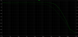
Please take a look to my last simulation of your last proposed schematic. It shows -3dB at 1MHz frequency response. Please enlighten me and tell me if this is OK or if it is too good a frequency response, when we are trying to avoid oscillations.
I will use this PCBs and then fully redesign them, after I can make them work. Even with the Zetex TO-92 transistors, I would like to use MJE340/350 and real heat sinks, with enough metal surface and a real hole to place a screw. On these PCBs (I have some 16 left) I would place the transistors from the bottom side to let me use some kind of heat sinking.
Please ask me whatever may be confusing, I don't like to make your valuable time be wasted. I appreciate it too much.
Thank you !
The problem is this:
My first schematics try to show exactly what my PCB does.
The designer (not me !!) made some terrible mistakes such as very small pads and very close pads, no space in between. This makes very difficult servicing and parts replacement without damaging the PCB. Believe me !
Now, your new proposed design , eliminated my last correction in which I included the missing Q7 and Q14. These are part of the original working PCB and I would like to follow this. Sorry for my fault. You made it right with my bad information.
So Q7 and Q14 are EFs. I found another mistake (my mistake while soldering SMDs) Q2 emitter had 33 Ohms instead of 330 Ohms as Q5 has, being a Wilson mirror. This may explain some disastrous behaviour.
So, finally, your suggestion should include EFs Q7 and Q14 of my last original schematic. Now I have 200 Zetex fresh units. It would be nice not to change the position of the trimpot if possible. I would have to drill the PCB and do some awful cabling. YES it nice to eliminate as much capacitors as possible not to alter the phase margin a lot. There is a network at G1 in the dual JFET. This cuts response at 1 Hz. What do you think about this ?
Please take a look to my last simulation of your last proposed schematic. It shows -3dB at 1MHz frequency response. Please enlighten me and tell me if this is OK or if it is too good a frequency response, when we are trying to avoid oscillations.
I will use this PCBs and then fully redesign them, after I can make them work. Even with the Zetex TO-92 transistors, I would like to use MJE340/350 and real heat sinks, with enough metal surface and a real hole to place a screw. On these PCBs (I have some 16 left) I would place the transistors from the bottom side to let me use some kind of heat sinking.
Please ask me whatever may be confusing, I don't like to make your valuable time be wasted. I appreciate it too much.
Thank you !
So sorry to have been away for too long. Haven't figured out a way to be more responsible, yet efficient, once I've stuck my big nose into someone's important work.😱
Sounds like excellent progress you've made. Good on ya'.
Its probably no longer of use to you, but here's where I was thinking of putting the couple of cheap diodes:
Good going!
Best Regards,
Rick
PS -- now I'll catch the rest of the way up from your post #69-ish.
Sounds like excellent progress you've made. Good on ya'.
Its probably no longer of use to you, but here's where I was thinking of putting the couple of cheap diodes:
Good going!
Best Regards,
Rick
PS -- now I'll catch the rest of the way up from your post #69-ish.
Attachments
Last edited:
OK, took me a minute to get caught up. Thanks for your patience.
On your recent post, some of the voltages have me puzzled. For starters, since they're 8 significant digits, they must have come from the simulator, yes? So before adding more confusion, I copied it and hacked in some notes.
Hope your customer appreciates the huge amount of excellent work you've put into this.
Cheers,
Rick
Attachments
I apologize in advance for my slow reaction ... my family member's health requires full attention.
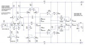
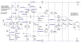
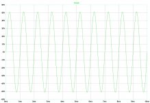
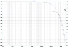
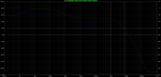
In the attachments you can see the schemetic, bode plot, stability, overload and overshoot at 1u//8 Ohms.
The idea is to make the most of the gm from the input J-fets, so I ran 5.1mA through each side (min. Idss is 5mA according to datasheet) and removed the source resistances and kept dissipation at ~ 225mW for both in the housing. At the same time, these currents are charge/discharge Miller compensation capacitors C1/C2, where C1 is also a feedforward capacitor that bypasses Q2 at HF. This compensation method allows a gain margin of ~ 19dB and a phase margin of 82°.
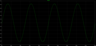
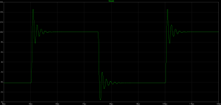
The picture of a 10Vp-p square 20kHz signal at 1u/8R load shows very good dumping, so (with ok PM and very good GM) a stable amplifier can be assumed.
So much for now from the amateur...professionals feel free to comment.🙂
In the attachments you can see the schemetic, bode plot, stability, overload and overshoot at 1u//8 Ohms.
The idea is to make the most of the gm from the input J-fets, so I ran 5.1mA through each side (min. Idss is 5mA according to datasheet) and removed the source resistances and kept dissipation at ~ 225mW for both in the housing. At the same time, these currents are charge/discharge Miller compensation capacitors C1/C2, where C1 is also a feedforward capacitor that bypasses Q2 at HF. This compensation method allows a gain margin of ~ 19dB and a phase margin of 82°.
The picture of a 10Vp-p square 20kHz signal at 1u/8R load shows very good dumping, so (with ok PM and very good GM) a stable amplifier can be assumed.
So much for now from the amateur...professionals feel free to comment.🙂
Attachments
-
 Goldmund 330 Clone Exicon sch.png68 KB · Views: 148
 -
 Goldmund 330 Clone Exicon bode.png13.1 KB · Views: 125
 -
 Goldmund 330 Clone Exicon phase and gain margines.png14.1 KB · Views: 97
 -
 Goldmund 330 Clone Exicon clipping.png13.6 KB · Views: 94
 -
 Goldmund 330 Clone Exicon overshoot 1u+8R.png9.6 KB · Views: 111
Dear aparatusonitus,
Can you kindly post the .asc file for others as a learning exercise ?
--gannaji
Can you kindly post the .asc file for others as a learning exercise ?
--gannaji
Um-m-m -- I don't think C1 can provide feed-forward because a cascode Emitter has so little voltage swing.😕
Nice work on the sims, too, but -- so many capacitors . . so much lag compensation.😱 Now up to 9, where previously we had 2 .. on some schematics 3?
I thought we had a bit of a consensus recommending the 10 or 15pF from Q2-Collector to J2-Gate (plus the usual VAS C-something, Base-Collector of Q2) -- at least unless/until the stability proves intractable.
Then again, mine is an amateur, non-professional opinion, too.😉
Get well wishes for your family member,
Rick
PS Thanks gannaji, that would be helpful . .and fun!😉
Last edited:
- Home
- Amplifiers
- Solid State
- Fixing and troubleshooting this MOSFET amplifier