So you would create the series and ground connections AFTER the limiters, letting the SMPS outputs float.
Ok, got it. Thanks.
I'll probably use the STP110N8F6 which is rated 80v and 110A with 6.5mOhm Rdson as I have a big tube of them already as employed on the SLB PSU's active bridge.
https://www.mouser.com/ProductDetai...5cJA9_BEky0s-SjlsKEhJNvPTeYG6I_hoC2KUQAvD_BwE
If the "Protective Earth" (3rd wire in the IEC mains connector) is separated from chassis ground, that makes me nervous.
The P.E. is connected to the chassis ground labeled "E" in the photos, and the "E" is connected to the 0v common via NTC 8D-20's as a ground loop breaker.
Last edited:
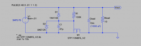
I found a Spice model for the STP110N8F6 and re-ran the simulation. Because of the lower Vgs threshold than my initial MOSFET choice, the time constant has to be longer to keep the inrush to a reasonable level. I am still modeling with a 1,000 uF load capacitance, but changed the supply voltage to 48 V.
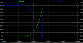
Here is a simulation with a 47 uF cap across the gate. The time constant is around 70 mS. The peak current through the MOSFET is 30 Amps under these conditions. Since you mentioned 800 Watt SMPSs, that should not be a problem for them.
Suggest you bench test this and try to capture the transient on a scope to validate the circuit. A current probe would be ideal, or a small resistor (<.1 Ohm) in series with the ground to measure the current.
Attachments
wtnh,
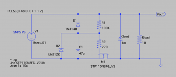
It is noted that 10mF is 10000uF, not 1000uF. You may also want to incorporate a gate stopper resistor.
It is noted that 10mF is 10000uF, not 1000uF. You may also want to incorporate a gate stopper resistor.
Oops - my bad - I changed the annotation but not the value. Thanks for catching that!
In that case, changing the load cap to actually be 1,000 uF (1m) reduces the MOSFET current to a measly 7 Amps peak. But the simulation still holds up with the larger capacitor value (10,000 uF), so there is plenty of margin for larger decoupling caps.
I was thinking about a gate stopper, but since the gate is connected to the source with a 47 uf cap, is this really needed? I suppose there is a small chance of oscillation in the linear region, but that is a transient condition. In any case, it would not hurt.
Thanks for catching that!In that case, changing the load cap to actually be 1,000 uF (1m) reduces the MOSFET current to a measly 7 Amps peak. But the simulation still holds up with the larger capacitor value (10,000 uF), so there is plenty of margin for larger decoupling caps.
I was thinking about a gate stopper, but since the gate is connected to the source with a 47 uf cap, is this really needed? I suppose there is a small chance of oscillation in the linear region, but that is a transient condition. In any case, it would not hurt.
Last edited:
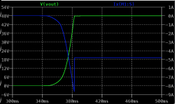
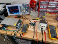
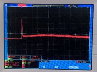
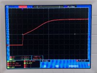
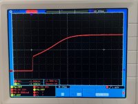
Here are the results of a test of the circuit proposed by Wtnh above. I used a 100uF cap instead of 47uF to give myself an even slower ramp up, I also added a 100nF 100v MKS bypass cap across the 100uF cap on the gate. I put a 0.1ohm 5w KOA BPR current sense resistor between the MOSFET drain and output 1000uF cap (Nichicon 63v). I used an EGB 300w 10ohm resistor with heatsink and the 800w SMPS was set at 49v output. There was 0.32v drop across the MOSFET at steady state (or about 1.5w dissipation - probably can use a small local heatsink). The transient pulses captured on the O-scope shows an initial in-rush spike of 18A and then it settles to the steady state value of 4.8A within 70ms. The voltage trace shows an initial sharp cliff of 20v followed by a gradual rise to the 48.8v steady state value in a little over 70ms. I then tested the SMPS directly connected to the 10ohm load and measured an almost identical voltage rise profile. So I am not sure if this soft start is doing anything to delay the ramp up any more than what the SMPS is already doing by itself?
Setup:

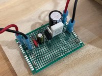
Circuit closeup:

If you noticed, I placed it on half of a veroboard that is all ready for a second rail to be added for a dual rail soft start.
Current (AC coupled voltage across 0.1ohm series R):

Would doubling the 47uF cap to 100uF cause the peak current to be 18A vs 9A as predicted?
Voltage output at load (DC coupled):

10ohm load connected directly to SMPS (no soft start circuit):

So I am not sure what to make of this. Maybe try adding a bigger capacitive load to see if it prevents the SMPS from going into hiccup mode?
Setup:
Circuit closeup:
If you noticed, I placed it on half of a veroboard that is all ready for a second rail to be added for a dual rail soft start.
Current (AC coupled voltage across 0.1ohm series R):
Would doubling the 47uF cap to 100uF cause the peak current to be 18A vs 9A as predicted?
Voltage output at load (DC coupled):
10ohm load connected directly to SMPS (no soft start circuit):
So I am not sure what to make of this. Maybe try adding a bigger capacitive load to see if it prevents the SMPS from going into hiccup mode?
Attachments
Last edited:
Looks like the SMPS already has a soft-start function built-in? If so, then the MOSFET circuit would be somewhat redundant. Is the supply going into stutter mode? Adding load capacitance should make it worse, not better.
I am ready to start on soldering up the All C's. I was thinking of starting in the middle of the pcb and working my way out to both edges. Would solder the big caps last. Sound good?
MM
MM
I find it easiest to divide them into groups of the same height and then solder a group at a time, starting with the shortest and working upwards. Place a book on top of each group and flip the whole thing over to solder. Or you can do all but the big electrolytics by bending the leads to keep them in place. One or two will usually slip and end up crooked, but the benefit is that if the last one isn't the value you need, then you've misplaced one of the others. Not infallible, of course.
Thanks for the info davidjt, I will be bending the leads and using a pcb vice, so no book needed.
MM
MM
I generally do any SMT parts first (if there are any), then I move onto smaller through hole axial resistors and DO-35 diodes. Then small radial film caps. Then TO-92, TO-126, TO-220 transistors, then large bulk caps. Finally power output transistors/MOSFETs (TO-247, TO-3P, TO-264 etc). It is helpful to go from inside to outside, but for the small axial leaded resistors, doesn't matter as I solder those from outside to in typically.
X,
Thanks for the info. One quick question before I get going. Are the 4 smd pads on the bottom required to be soldered for proper operation, or are they optional if you solder the thru hole caps on the top side. I "thought I read" that JPS was designing optional smd on the bottom, but this may have been for theFH9HVX, rather than the All C's. Just checking to ensure less problems.
MM
The SMT caps are optional in case you don’t use the TH ones on the other side. Some people believe that small NP0 or C0G compensation caps sound better than larger TH ones.
Solder paste on one end of pad, place the device, hold with tweezers, heat paste with iron or air, then do the other end. Sound OK?
I would do the above for practice, as I have never tried smd soldering. If I mess it up, I can still use TH. Correct?
MM
I would do the above for practice, as I have never tried smd soldering. If I mess it up, I can still use TH. Correct?
MM
Yes, hot air will melt both ends at once. If gentle air no need to hold with tweezer. It’s very simple. If make mistake remove with iron chisel tip or hot air.
Thanks X,
I am a bit confused with what components are needed for the " chassis" connections shown on the All C's BOM. I see where the R131 & C132 are placed. I do not know what component goes in the PE spot (I assume PE means protective earth). I also do not know what X131, is so I can search for it. A picture of this set up would be great if possible.
Thanks,
MM
If you go to the listing on my Etsy shop, you can find the stuffing diagram and 3d render. X131 is the protective earth Faston tab.
X,
Thanks for the info. I was confused, on my pcb and on the pcb on your website, X131 is marked as PE. On the stuffing diagram it is X131, rather than PE. I guess I need to enhance my schematic reading skills. The 3D rendering does not show a faston at all for X131.
So I would connect a wire from the X131 faston to the chassis for the protective earth?
- Home
- Group Buys
- FH9HVX - Budget Conscious 100w Class AB for Lean Times