yes i know...2SD 669 and 2SD 669A(180V) is available
but that has nothing to do what the group of hfe B, C, D you get...
but that has nothing to do what the group of hfe B, C, D you get...
Hi Chris,
with my little knowledge i would choose BD types. I often have seen instead of H669/BD139...
In my thougt the 2SD are not critical.
Instead of 2SC2240 i can use KSC1845.
The world is colourful.... 🙂
Greets
Peter
with my little knowledge i would choose BD types. I often have seen instead of H669/BD139...
In my thougt the 2SD are not critical.
Instead of 2SC2240 i can use KSC1845.
The world is colourful.... 🙂
Greets
Peter

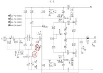
I am dropping the TMC scheme because sim results shows different profile values when compared with the original. It has become a different amplifier in comparison, so I am sticking to almost the same values as with FH8/FH9. Three devices was added in my circuit, two 1n4004 diodes as additional protection for the outputs and one led for thermal tracking.
Attachments


Hi @Kleinhorn
Have you received your PCB from post 106 ?
Did you get a chance to assemble a set and test them ?
Thanks
Eric
Have you received your PCB from post 106 ?
Did you get a chance to assemble a set and test them ?
Thanks
Eric

Hi,
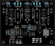
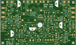
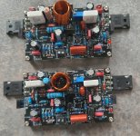
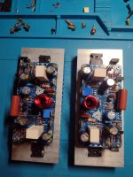
i began to assemble, because i wanted to know if all components fit well....
I have to give a little more space to the feedback capacitor...
I changed the footprint of one zobel resistor, made it bigger. The pot had moved a little bit...
The rest is ok. You can see on the picture the older, first version.
I will post changed gerber files...sorry...The 3d look of Kicad has sometimes nothing to do with the reality...
Greets
Peter
Attachments
Hi,
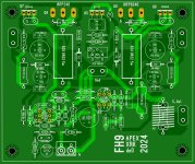
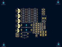
i have some footprints changed now to get get more space to other components. I post a new gerber file. If someone is in a hurry he can use the older prasi board.
I dont know how long it will take to test my pcb.
Greets
Peter
i have some footprints changed now to get get more space to other components. I post a new gerber file. If someone is in a hurry he can use the older prasi board.
I dont know how long it will take to test my pcb.
Greets
Peter
Attachments
Last edited:
Hi..
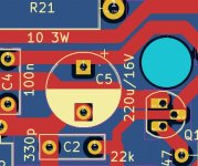
I have compared the components with the boom list. The 1000 µf feedback capacitor has to change to 220µf/16 Volt in this variation with led. No other footprint, only a wrong value in the gerberfile. If you want to use my pcb think about this change....
XRK used a vishay led, i also do.
Good night
Peter
Attachments
Hi Peter
your work is fine.
(do you have interests to do a small dual side pcb for FX8....kisses chris 😉😆 )
Should that cap not be as big as possible?
your work is fine.
(do you have interests to do a small dual side pcb for FX8....kisses chris 😉😆 )
Should that cap not be as big as possible?
Hi Chris,
in the boom and schematic are two different variations.
1. With 2x1n4148 capacitor and other connecting...1000µf.
2. With led insert the capacitor changed to 220µf.
Its can also been seen in the different schematics. I think the second schematic XRK using for its pcb's, he offers.
The footprint on my pcb is the same, 8mm dia.
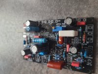
My Pcb are fully assembled. Testing is missing...
Peter
in the boom and schematic are two different variations.
1. With 2x1n4148 capacitor and other connecting...1000µf.
2. With led insert the capacitor changed to 220µf.
Its can also been seen in the different schematics. I think the second schematic XRK using for its pcb's, he offers.
The footprint on my pcb is the same, 8mm dia.
My Pcb are fully assembled. Testing is missing...
Peter
Attachments
yes you are right...in the FH9 HVX is a 220µF cap too.Hi Chris,
in the boom and schematic are two different variations.
1. With 2x1n4148 capacitor and other connecting...1000µf.
2. With led insert the capacitor changed to 220µf.
Its can also been seen in the different schematics. I think the second schematic XRK using for its pcb's, he offers.
The footprint on my pcb is the same, 8mm dia.
My Pcb are fully assembled. Testing is missing...
Peter
FX8 is a single sides layout pcb...this is the reason why is so big. your and prais layout of FH9 is compact and very small so build a 2U housing amp is possible
THT dual layer would be nice...if you like the sound.
but post this in FX8 thread please
thx
chris
THT dual layer would be nice...if you like the sound.
but post this in FX8 thread please
thx
chris
I personally like sound of FH9 over FX8. LatFETs don’t have as good bass authority as HexFETs in my experience - probably impedance in On state is not as low as HexFET. The latFETs are also very pricey.
Yes the voltage that drops over one 0,22 resistor.
My second amp has a biasing of 80 mA because the heatsinks are smaller. If i remember right 70 mA is the minimum for biasing the transistors right.
You will see how hot your heatsinks will get if the amp works for half an hour. With bigger heatsinks i have choosen 120 mA but more is possible...
mV/0,22 (22mV/0,22= 100 mA) to get 120 mA adjust 26,5 mV.
If you make the measurement short the input and without any load at the output...
Second possibility as Prasi wrote...(for the FX8)
1. you will need 2 nos. of 10ohm 1W/2W resistors.
1a. turn the trim pot so that resistance between first and third leg of trimmer is approx 500 ohm. (half 1K in this case)
2. Connect one lead these 10ohm resistors in series with your + and - rail wires of psu.
3. connect the other lead of resistors to amplifier +/- supply connector on amp pcb.
4. switch on supply and measure the voltage drop across these rail resistors.
4a. measure the voltage between spk out and ground. this is offset. it should be less than +/-30mV. Good matching of Hfe of i/p transistor pair (Q1/Q3) will ensure that offset is close to zero.
5. total quiescient current is given by I= V/10ohm
6. set the pot so that voltage drop across 10 ohm rail resistors is about 1V to 1.1 V.
7. Let the amp warm up for 1/2 an hour recheck the bias
8. Adjust pot if required to have voltage drop of 1 to 1.1 V.
9. This will ensure that you get a bias through o/p stage of approx. 100mA.
and so on...
Peter
Last edited:
- Home
- Amplifiers
- Solid State
- FH9 XRK mod