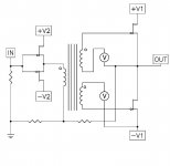
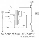
At the risk of ignoring my dads advice ( "no one knows how big a fool you are until you open your mouth"...) it appears to me that the phase is correct as presented in the schematic.
... If the output haves were effectively outputing the same signal, there would be no F.B. If one is distorted and the other not, there would be F.B. correcting the distortion
Like the master, I'll try quoting myself. 😀 In the previous post I did not mean the 2 1/2s of the output were outputing the same signal. I meant, if they were opposite in phase but the same level and undistorted. They cancel!
Same phase relationships as in the OTL schematic shown in thread #38. Thus, the signal drives to the FETs in F6 are Out of phase.At the risk of ignoring my dads advice ( "no one knows how big a fool you are until you open your mouth"...) it appears to me that the phase is correct as presented in the schematic.
Why is everyone debating whether the phase is correct? Obviously it functions properly. It wasn't designed by a beginner.
Last edited:
lalala
possible variations
all with different amount of Zen
some having Mu , some uM , some MuuM

edit : added original Pa's (with title ) sch , redrawn slightly , for easier comprehension
possible variations
all with different amount of Zen
some having Mu , some uM , some MuuM
edit : added original Pa's (with title ) sch , redrawn slightly , for easier comprehension
Attachments

Last edited:
Like the master, I'll try quoting myself. 😀 In the previous post I did not mean the 2 1/2s of the output were outputing the same signal. I meant, if they were opposite in phase but the same level and undistorted. They cancel!
exactly why I'm
 all the time , surprised to the bone
as I wrote , only logical way , to stay on same path , is that upper modulation is attenuated in some way
but , I will not be surprised if Papa say tomorrow that there is ( intentional or not
) mistake on schematic , in secondary phasing 
So the transformer has become the modulation point.
more apparatus then point
one detail is indicative - existence of +/-V1 and +/-V2
What are you getting at? I just thought those input JFETs are a low voltage and a high current. Or maybe there is a pair of 'em for low low source impeadance for the xfrmr. This is good or the JFETs but bad for output power. So, there is a bigger supply for the output.
one detail is indicative - existence of +/-V1 and +/-V2
Not understanding completely, but are you referring to a normal circlotron and the presence of 2 sets of rails. It seems we are accomplishing this with a single set and the transformer.
@ flg
input ones are small Toshiba's , without doubt
think M2
@ Buzz
dunno - just came to my mind that there is either :
- inserted reg (or filter) for input stage , fed from common FW PSU (+/-22Vdc) , or
- there is separate PSU for output stage , with higher voltage than common FW PSU
I'm just mudding the water now , have no slightest clue what Papa is thinking ...... except that he's having major laughing time ......
😉
Last edited:
Mr. Pass may have had a trick up his sleeve.Why is everyone debating whether the phase is correct? Obviously it functions properly. It wasn't designed by a beginner.
exactly why I'm
as I wrote , only logical way , to stay on same path , is that upper modulation is attenuated in some way
but , I will not be surprised if Papa say tomorrow that there is ( intentional or not
zm.... good catch on V2 and V1. What this is for we can only guess at huh ?... from the clues so far, (4*600ohm windings) it would seem that the primary is two 600 ohm windings in parallel ... with each secondaries 600ohm each also, this doesn't give any voltage gain...more thinking to do here ...
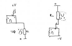
Anyway, seperately, with respect to the phase of the secondaries, this is how i look at it ... i looked at the inputs relative to the phase dot on the tx secondaries, and for the outputs, relative to 0v (hence i drew in the eyes lols) ... if my feeble mind if correct, that means the outputs DON'T cancel each other out if the fets are driven in the way indicated by the schematic in post 1......
now how do we think about that feedback loop and unequal voltage gain for top and bottom device .........

Attachments
Help..... so many bees are humming! That I cannot hear my own voice......😎
What?
 Ich Verstae sie nicht Generg
Perhaps???
I know NP said 4 600 ohm windings, unless the input is wired in series or something...Looks like one of these per channel fits the schematic in the first post.
I know NP said 4 600 ohm windings, unless the input is wired in series or something...Looks like one of these per channel fits the schematic in the first post.
Perhaps???
I know NP said 4 600 ohm windings, unless the input is wired in series or something...Looks like one of these per channel fits the schematic in the first post.
possible i guess but series connection of the primaries would make the tx setup a step-down (ungain stage ?) but then again with NP, you never know 🙂
What?
Thanks flg! It is a pleasure to follow the discussion, unfortunately beyond my horizon.....😀
zm......
few mistakes :
- smilies on your schm are not smiling 😉
- think what's happening in output mode ........ your analysis is wrong for one half of output ; as drawn in post one sch ,they're exactly the same
btw. world is full with 600:600 xformers ,where each winding is CT , so effectively having 4 x 150R windings
it's extremely hard to find 4x600R xformers anywhere .......
Last edited:
- Home
- Amplifiers
- Pass Labs
- F6 Amplifier