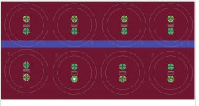
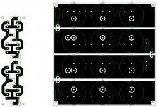
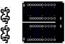
Not really sure, but geometrically it looks correct. I think there is some problem with the tracks on one layer. It is unusual to have both pins isolated on any given plane, so double check everything.
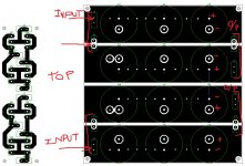
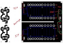
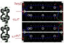
Here's an rough-and-ready example created in 5 minutes in Eagle for you to start from. All the alignments are slightly off, this is just conceptual.
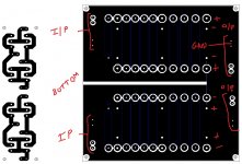
Notice each cap is connected to alternate layers for rail and return. I drew the returns on bottom layer and the rail on the top, but in your case since you will need access to the rail layer, you should flip them over.
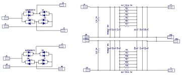
The drawing program should automatically know where to connect each component depending on how they are joined in the schematic, including your quick connect tabs.
Note bottom layer is a continuous unbroken layer from the top left corner to bottom right corner.
Attachments
In post42, the two traces for power rails can be brought closer together. A gap of 0.5mm would be appropriate.
The input from the Transformer+Rectifier is at one end. The output to the client circuit if from the other end.
The input from the Transformer+Rectifier is at one end. The output to the client circuit if from the other end.
Please check cap polarity.
Top row of caps is input.
Lower row of caps is output.
You do not want them to be closer together as that will couple the input to output at higher frequencies.
There will be resistors between the two rows, under the board.
This is one power supply rail.
Will have to be duplicated for other rail.
Besides there are a few unconnected nodes etc, this is a pictorial example not the final layout (hopefully).
That does not show on the PCB.Please check cap polarity.
Top row of caps is input.
Lower row of caps is output.
You do not want them to be closer together as that will couple the input to output at higher frequencies.
There will be resistors between the two rows, under the board.
This is one power supply rail.
Will have to be duplicated for other rail.
Besides there are a few unconnected nodes etc, this is a pictorial example not the final layout (hopefully).
You will have to mark on the PCB where the input is and where the output is, otherwise a Builder will interpret it in any of many different ways.
I did !
Andrew
We've had these kind of exchanges many times, when you fail to reference the post to which the answer was made, and the layout that this builder did. And then use bluster to cover your oversight or mis-information. Recently you did this on the JFET checking thread, which I declined to respond to, and now here.
I cannot pander to your whims and fancies. Please read posts and understand the context of the thread. These are conversations, and one post always stems from another. No post can be taken in isolation like you are doing, and you do this on almost every second post of mine. I hate to put someone like you on an ignore list but I think it's now time. What little respect I had for you is slowly ebbing away when you act like a child. Which I know you're not.
I don't know what language you are conversant in but this is the first line of post 42, written in what I know was English:
If you like, I can translate this into multiple languages using Google Translate, please indicate which one works for you, Swahili, Mandarin, or whatever it is you happen to understand.
Please READ posts and don't just shoot off comments on just looking at the picture. We have been orienting the capacitors exactly like this for the last ten posts in the thread, if you didn't notice or didn't look or didn't care or didn't remember, that's not my problem. YOU are supposed to re-familiarise yourself with the conversation, if required compare older pictures and layouts. YOU have to do it BEFORE typing. If the builder is confused, LET HIM ASK! Do not get it into your head that if you don't get it, no one else will.
Good day to you, Sir!
We've had these kind of exchanges many times, when you fail to reference the post to which the answer was made, and the layout that this builder did. And then use bluster to cover your oversight or mis-information. Recently you did this on the JFET checking thread, which I declined to respond to, and now here.
I cannot pander to your whims and fancies. Please read posts and understand the context of the thread. These are conversations, and one post always stems from another. No post can be taken in isolation like you are doing, and you do this on almost every second post of mine. I hate to put someone like you on an ignore list but I think it's now time. What little respect I had for you is slowly ebbing away when you act like a child. Which I know you're not.
I don't know what language you are conversant in but this is the first line of post 42, written in what I know was English:
Here's an rough-and-ready example created in 5 minutes in Eagle for you to start from. All the alignments are slightly off, this is just conceptual.
If you like, I can translate this into multiple languages using Google Translate, please indicate which one works for you, Swahili, Mandarin, or whatever it is you happen to understand.
Please READ posts and don't just shoot off comments on just looking at the picture. We have been orienting the capacitors exactly like this for the last ten posts in the thread, if you didn't notice or didn't look or didn't care or didn't remember, that's not my problem. YOU are supposed to re-familiarise yourself with the conversation, if required compare older pictures and layouts. YOU have to do it BEFORE typing. If the builder is confused, LET HIM ASK! Do not get it into your head that if you don't get it, no one else will.
Good day to you, Sir!
I am not having a dig at you. I was not criticising your helpful post.
I was trying help the enquirer by giving a bit more information to help him towards a better layout.
The two messages in my post were:
try closing up the gap
and
place the input at the opposite end from the output.
I got the output in the wrong place. That is my mistake.
But my mistake does not change the message. The philosopy is small loop area and keep the output away from the input.
Sangram, wording apart you should check the caps polarity unless you are going to get a double positive output. Which is not the case for F5T.
Where is the ground plane supposed to be on your drawing?
Currently you have both caps minuses on the center which supposed in be a ground plane
Which does not correspond yo commonly used design and may cause confusion.
Sent from my ONE A2003 using Tapatalk
Where is the ground plane supposed to be on your drawing?
Currently you have both caps minuses on the center which supposed in be a ground plane
Which does not correspond yo commonly used design and may cause confusion.
Sent from my ONE A2003 using Tapatalk
Hi
Andrew, I owe you an apology for my intemperate response.
Aradan, you have to go back to the beginning of the thread to understand the logic. The TS has four row of capacitors on his layout, this is an illustration of one half of that. The resistors are under the board.
More specifically, this is a response to post 40 where I noticed that the layout had isolated both terminals of the capacitors from the plane, which obviously is not right. I mentioned it in post 41, then thought to provide a quick example to demonstrate one way (not the only way) to achieve this in his layout.
My picture was an attempt to illustrate *the connection of capacitors to opposed planes* and nothing else.
Again, if you follow the thread, the post makes sense, and not if you see that picture in isolation and assume it is a complete supply. It is not. It never was, and never intended to be, and very clear from the wording of the post.
I am opposed to spoon-feeding and expect the TS to understand my post in context of the conversation, and for other readers to follow the conversation and try to analyse why something was done the way it was done - not just pointing fingers and saying why it is wrong.
I know it is wrong, the F5T requires bipolar supplies - I know that and most people with an inkling do so as well. A disconnect like that should be investigated and understood. It's quite possible I'm an idiot, but maybe there's more to it. If I am expected to provide complete power supply layouts in every post, then probably I'm in the wrong forum, or someone else is.
I'm sorry if that sounds rude. But that's just how it is. We are expected to read complete threads, even when they stretch over 100 pages. I make the effort, as should everybody else.
guys blame it on me for not posting detail information. Please check images.
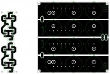
Tried what i wanted to achieve
1. Have thick tracks.
2. 0V tracks below supply tracks(Top are supply and bottom is all 0V plane)
Please have a look and let me know if i have made any mistake like before(post#27) or a new one 🙂
- Planes have 3mm seperation
- 1mm gap between pads and planes, let me know if it is too less.
- cap/resistor pads are 6mm dia.
Thankyou Marce, Sangram and Andrew for helping me with this.
Attachments
Last edited:
Hi CJS
You can simply take the ground output from the joint between the two return planes topside. No need for external joining.
I would also suggest flipping the two planes, with the rails on the underside and ground topside. This will make the process of soldering the resistors easier and prevent the chance of accidental shorting the pads to the ground plane.
Hi CJS
You can simply take the ground output from the joint between the two return planes topside. No need for external joining.
I would also suggest flipping the two planes, with the rails on the underside and ground topside. This will make the process of soldering the resistors easier and prevent the chance of accidental shorting the pads to the ground plane.
Since Ground planes are already joined not doing any external joining.
As for flipping, i probably will.
Question on thermals, since lot of current is to flow aren't we introducing more problems with thermals?
sorry, a very basic question but i don't know
How do i remove my previous attachments that are not correct and could mislead someone?
Last edited:
Hi
You can beef up thermals like the attached. NOTE: Track is not routed anywhere, it is drawn for reference only!!
I do that by routing the tracks first, then making the plane and connecting it to the respective net. It is possible with a thick enough track to totally eliminate the thermal, I do this for lugs and tabs which are basically lumps of metal and do not mind a few extra seconds of soldering heat.
For anything that needs higher current, I try to reach a decent balance between current capability and thermal relief. Often a hybrid model works, where one side (solder side) is relieved from the plane and the other side (component side) is used for the track.
Attachments
Since Ground planes are already joined not doing any external joining.
I see 4 tabs on the output side, 2 connected to the ground plane and one on each output rail. Were you planning to take the supply common of one channel from one tab and the other for the other channel? If so, you will have severe crosstalk issues because the return currents for each return will be totally mixed.
Move both ground tabs to the middle, so the current flow equally in both directions. A few mm of separation is not a problem but the 3" or so you have now is quite bad.
RightI see 4 tabs on the output side, 2 connected to the ground plane and one on each output rail.
Not sure if i got you.Were you planning to take the supply common of one channel from one tab and the other for the other channel? If so, you will have severe crosstalk issues because the return currents for each return will be totally mixed.
J13 (+V, top only)
J16 (Connected to ground/0V plane , bottom)
J14 (-V, top only)
J15 (Connected to ground/0V plane , bottom)
Now my ground/0v plane is at bottom and connected towards right side(output side at bottom).
(J13,J16) goes to one client circuit
(J14,J15) goes to other client circuit
current return paths are separate for each client circuit and merge at bottom right side of 0v plane.
If i move the ground connectors to the middle(marked by green arrow) i will be moving away from blue rectangle, isn't that bad ?Move both ground tabs to the middle, so the current flow equally in both directions. A few mm of separation is not a problem but the 3" or so you have now is quite bad.
Attachments
Last edited:
Hi CJS
Are you taking a four-wire power connection to the amplifier or three-wire?
If you are taking four wire connection you need not connect the two halves of the return plane together (as they will be properly merged on the amplifier PCB) and your connection method is fine.
If it is a three-wire connection, then the 15/16 should move to the middle/between tab 13/14. I would also (personally) simply merge the two return planes together in such a case, creating one large continuous copper area.
Hi CJS
Are you taking a four-wire power connection to the amplifier or three-wire?
If you are taking four wire connection you need not connect the two halves of the return plane together (as they will be properly merged on the amplifier PCB) and your connection method is fine.
If it is a three-wire connection, then the 15/16 should move to the middle/between tab 13/14. I would also (personally) simply merge the two return planes together in such a case, creating one large continuous copper area.
Sorry for messing up.
Making it 3 wire.
Moved J13 (+V, top only) and J14 (-V, top only) to corners and J15,J16 (GND/0v) close towards middle.
-Two wires from J13 will go out , one to left channel and one to right channel
-Two wires from J14 will go out , one to left channel and one to right channel
- Two wires will go out from J15, one to left channel GND, one to right channel GND and J16 to thermistor > mains supply earth ground.
Also signal input GND will be connected to J16
Attachments
Last edited:
Hi
I wouldn't flip input and output like that.
As has been said by Andrew before, you need to keep loop area small. Loop area is the physical distance between currents, and this is a function of PCB routing - not the schematic which is more theoretical. For example, in the schematic you can connect 'ground' anywhere, but in a PCB the distance between - and size of - traces makes a material difference in circuit operation.
Which means you should just put the rail output tabs close to the ground tabs. The input side was also okay earlier, the only change required was to put the ground tabs where you have them now.
Hi
I wouldn't flip input and output like that.
As has been said by Andrew before, you need to keep loop area small. Loop area is the physical distance between currents, and this is a function of PCB routing - not the schematic which is more theoretical. For example, in the schematic you can connect 'ground' anywhere, but in a PCB the distance between - and size of - traces makes a material difference in circuit operation.
Which means you should just put the rail output tabs close to the ground tabs. The input side was also okay earlier, the only change required was to put the ground tabs where you have them now.
Reverted to where i was earlier, just moved (GND/0V) tabs to middle.
it was getting congested, so removed J16, all GND will go out from J15.
Attachments
Looks okay to me, you can crimp two cables on each connector with no issues, I do that all the time.
Don't forget that you should be moving the rail side to the bottom (ground planes are topside) to make soldering of the resistors a bit easier. It is manageable both ways though, you can execute as per your wish.
Don't forget that you should be moving the rail side to the bottom (ground planes are topside) to make soldering of the resistors a bit easier. It is manageable both ways though, you can execute as per your wish.
- Status
- Not open for further replies.
- Home
- Amplifiers
- Power Supplies
- f5 Turbo power supply
