hi Sangram/Andrew,
Implemented changes you suggested the best possible way i could.
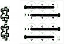
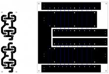
Separated diode board, caps lined up and resistors go under. +/- tracks on both layers.
Thankyou
Implemented changes you suggested the best possible way i could.
Separated diode board, caps lined up and resistors go under. +/- tracks on both layers.
Thankyou
Attachments
Last edited:
Hi CJS
That looks a sight better.
However I would turn the caps 180 degrees so that the "grounds" are all closely coupled. That minimises the eddy currents and may help you get rid of (if you want) the plane.
The resistors' leads become slightly longer but that is not going to be an issue.
That looks a sight better.
However I would turn the caps 180 degrees so that the "grounds" are all closely coupled. That minimises the eddy currents and may help you get rid of (if you want) the plane.
The resistors' leads become slightly longer but that is not going to be an issue.
Hi CJS
That looks a sight better.
However I would turn the caps 180 degrees so that the "grounds" are all closely coupled. That minimises the eddy currents and may help you get rid of (if you want) the plane.
The resistors' leads become slightly longer but that is not going to be an issue.
If i rotate all of them 180 degrees, i'll have to widen resistor mounting holes to align it to cap, resistors with long leads , is that good?
By plane you mean the copper pour on back of PCB(connected to ground)?
Is plane a bad idea?
Also if i get rid of copper pour and connect grounds using traces, i'll have to reduce width. Currently it is 10mm both top and bottom.
Last edited:
Hi
Lengthening of the resistor leads is not an issue. We are adding resistance anyway (if that's your worry).
Plane is not a bad idea, it's probably not necessary. Since you haven't provided thermal relief it could be a problem while soldering (in this instance) but either way it shouldn't make a difference if your tracks are nice and thick.
I personally use at least 30-35mm for these kind of applications, and if that's not possible I use some braid to help. The braid is soldered directly to the cap pins, not the copper. You can use the restrict layer to block off the solder resist and solder the braid on the exposed tinning.
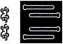
Don't think about trace versus plane the way you are. Those are the software functions. Use large copper areas that will approximate a plane. One nice thick central 'track' with caps feeding off it. I've attached an example picture. Thrown together in eagle in five minutes so alignment etc are a little off, this is just to show you an example - not a recommendation.
Lengthening of the resistor leads is not an issue. We are adding resistance anyway (if that's your worry).
Plane is not a bad idea, it's probably not necessary. Since you haven't provided thermal relief it could be a problem while soldering (in this instance) but either way it shouldn't make a difference if your tracks are nice and thick.
I personally use at least 30-35mm for these kind of applications, and if that's not possible I use some braid to help. The braid is soldered directly to the cap pins, not the copper. You can use the restrict layer to block off the solder resist and solder the braid on the exposed tinning.
Don't think about trace versus plane the way you are. Those are the software functions. Use large copper areas that will approximate a plane. One nice thick central 'track' with caps feeding off it. I've attached an example picture. Thrown together in eagle in five minutes so alignment etc are a little off, this is just to show you an example - not a recommendation.
Attachments

Last edited:
Hi
Lengthening of the resistor leads is not an issue. We are adding resistance anyway (if that's your worry).
Plane is not a bad idea, it's probably not necessary. Since you haven't provided thermal relief it could be a problem while soldering (in this instance) but either way it shouldn't make a difference if your tracks are nice and thick.
I personally use at least 30-35mm for these kind of applications, and if that's not possible I use some braid to help. The braid is soldered directly to the cap pins, not the copper. You can use the restrict layer to block off the solder resist and solder the braid on the exposed tinning.
Don't think about trace versus plane the way you are. Those are the software functions. Use large copper areas that will approximate a plane. One nice thick central 'track' with caps feeding off it. I've attached an example picture. Thrown together in eagle in five minutes so alignment etc are a little off, this is just to show you an example - not a recommendation.
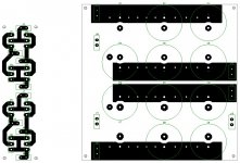
Thank you Sangram.
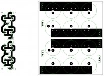
Rotated caps, is rectangular shape fine?
There is 3mm gap between any two copper areas
For +/- top and bottom layer doesn't overlap 100% as in bottom layer i have ground area and had to keep 3mm spacing between any two copper areas.
Will add thermal relief, i understand it will be frustrating while soldering since i don't do lot of soldering.
Attachments
Last edited:
3mm spacing is fine. I'm not too fond of right angles in PCBs except the board outline. Rounded or tapered corners look better and avoid current crowding (though I think in this case it is not going to be an issues.
Consider using large cement 5W resistors for the R, that way the body will span the length naturally. Also you can bolt it directly to the case floor to keep them at a consistent temperature. They will both provide PCB spacing, and stay cool. Use a silicon insulator underneath to ease pressure if required, or a soft foam rubber between the PCb and the resistors. Too much mounting pressure applied unwittingly will crack them.
Good Luck!
3mm spacing is fine. I'm not too fond of right angles in PCBs except the board outline. Rounded or tapered corners look better and avoid current crowding (though I think in this case it is not going to be an issues.
Consider using large cement 5W resistors for the R, that way the body will span the length naturally. Also you can bolt it directly to the case floor to keep them at a consistent temperature. They will both provide PCB spacing, and stay cool. Use a silicon insulator underneath to ease pressure if required, or a soft foam rubber between the PCb and the resistors. Too much mounting pressure applied unwittingly will crack them.
Good Luck!
Thankyou Sangram.
I am uploading it for anyone who wishes to use it. It was created using dip trace.
Caps are 35mm dia
Diodes are ON Semi MUR
Attachments
Last edited:
You have a problem.
The connected planes need a connection to the transformer. That is the input side of the commoned planes.
The connected planes need a connection to the client circuits. That would be the output side.
The output side must NOT be connected to the input side.
You must NOT take the PSU Zero Volts (for the client circuits) from the charging circuit connections.
Hi Andrew,You have a problem.
The connected planes need a connection to the transformer. That is the input side of the commoned planes.
The connected planes need a connection to the client circuits. That would be the output side.
The output side must NOT be connected to the input side.
You must NOT take the PSU Zero Volts (for the client circuits) from the charging circuit connections.
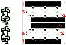
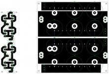
Not sure if i got you, if you look at attached images.
I have a diode board on left from where 1,3,5 and 6 will come.
2 = V+
4 = V-
7 = GND
Attachments


1 & 5 are the input from the transformer. This is the charging part.
2 and 7 are the output to feed the client circuit.
You have moved 7 around and into the charging side.
3 & 6 are the inputs and 4 and 7 are the outputs is the charging side separated from the DC side?
Just hardwire from transformer to input with a twisted pair. Then from C1 to C2 with a twisted pair, Then from C2 to Resistors with a twisted pair then from resistors to C5 with a twisted pair, then from C5 to C6with a twisted pair and finally from C6 to load with a twisted pair.
Then repeat for the other half.
Hi CJS,
The issue is that the return currents moving between the upper half of the board and the load will have to travel all the way through the lower half as well.
7 on the schematic illustrates the correct way of doing this, you have joined 5 and 6 instead and routed the output return to the top of C5 (?). The extent of the problem is easier to visualise if you imagine the return path to the load from C3. It's a pretty long route and flows among a lot of other mixed currents. In truth you will always have one cap very far from the load, but we're still trying to optimise.
Keep the returns separated and join them at the output side, not the input side. You can achieve this by mirroring the C-shape, where the solid joint between the two halves moves to the right side (output side) of the board. Take the output from the center of the vertical portion of the 'C'.
Thus each rectifier and cap bank sees its own return, and the output side sees the sum of both returns. You may need to shift your tracks a bit. Don't be scared of using one massive polygon if it helps, your program should automatically isolate the cap pads if they are not to be connected to that polygon.

The supply tracks should be over the 0V tracks/plane to couple them capacitavly and reduce inductance, broadside coupled...
hi Andrew/Sangram,
Which is better
to have supply track over 0v track and with 17mm supply track on one side only
Vs
17mm supply track on both side and no supply-0V overlapping.
Track Thickness Vs supply/0v Overlapping?
Which is better
to have supply track over 0v track and with 17mm supply track on one side only
Vs
17mm supply track on both side and no supply-0V overlapping.
Track Thickness Vs supply/0v Overlapping?
Sorry for jumping in. Did anyone try the CLC filter in the PSU for F5T, was wondering whether there are some values of the L already tested for F5T 🙂
the PSU requires low inductance and high capacitance.
That means the traces need to be very close together.
Twisted pairs, or two planes with traces directly one over the other can acheive that.
The spacing between a two plane 1.6mm PCB is about the same as two thick insulation wires twisted together.
The wide plane traces will have less inductance than the circular wires of a twisted pair.
1.16mm diameter hook up wire used as a twisted pair has a core to core spacing of ~0.56mm. That reduces the inductance as well as reducing the emitted EMI. Cat5 or cat6 will have even closer core to core spacing. If the ~0.5mm diameter cores suit your current demands, then it too will perform very well.
Last edited:
If you want to follow marce's suggestion, you can move supply and return tracks to opposite sides of the board and thicken them to approximate opposed planes.
There is no need to choose, you can achieve both.
There is no need to choose, you can achieve both.
100T of 1mm diameter enameled copper wound on a 20mm bobbin gives an air core inductor ~40mm diam by 10mm wide.Sorry for jumping in. Did anyone try the CLC filter in the PSU for F5T, was wondering whether there are some values of the L already tested for F5T 🙂
Works very well as the R+L between two banks of C & C.
Thankyou Andrew/Sangram.
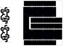
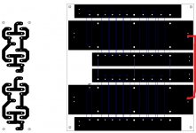
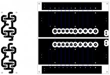
something like this?If you want to follow marce's suggestion, you can move supply and return tracks to opposite sides of the board and thicken them to approximate opposed planes.
There is no need to choose, you can achieve both.
Attachments
- Status
- Not open for further replies.
- Home
- Amplifiers
- Power Supplies
- f5 Turbo power supply