Still at work so no much to say apart from the big reason behind the current voltages W out discussion.
I was thinking to get an Idea of the currents on the drain traks
I know I can get 1 or 2 ounces copper boards 3 or 4 be a bit more difficoult
Sems like You have a 260mm long trak on the speakers so one would calculate the track thikness
If you use the diodes and plan on loads of current maybe a "buss bar" is needed there
maybe a "buss bar" is needed there
I could actually lay a track on both sides of the board for the output.
Adcom used a bus-bar -- easily made from the brass stock you can get from a hobby supply store.
As its DIY you needn't be hyper-fussy about the board width.
As its DIY you needn't be hyper-fussy about the board width.
Well, I've made the output two sided.
Final cut maybe?
Final cut maybe?
An externally hosted image should be here but it was not working when we last tested it.
Last edited:
Wrong image previously. Here's the correct one
An externally hosted image should be here but it was not working when we last tested it.
<snip>
I was planning to put mounting holes on the PSU.
<snip>
Would it be possible to have the CL30 thermistor and C1 on the power supply board as well please, plus the CL60 and connections for the bridge rectifier ground loop isolation? On the F5 I built, the CL60 for ground loop isolation is on the psu board but the one for surge protection and small DC filter cap aren't, and as a consequence are not (yet) very neat (I'm ashamed to say).
BTW the layouts are looking really nice
cheers
Nick
Nick,
I could do, but it might be better on a small separate board as I don't imagine many would want to do it that way.
Something like this......
An externally hosted image should be here but it was not working when we last tested it.
Andy
Wish you would make fatter pads for the small components and beef up the traces wherever there is real estate available - if necessary make the board slightly wider, as there is no mandate to keep the board this width? (width being the shorter distance)
Example, fatter pads and traces for C6, R14 (etc.) and I like to use 1/2 watt resistors over 1/4 watt. Also Q6/7 no need for tiny pads? If you blow them or want to experiment with different devices, the smaller pads get WAY hotter when desoldering and cool slower... Also I might consider moving the buss that goes to the gate resistors centered under the power resistors, AND making more pin spacings available for the power resistors, since I would use Vishay or Caddocks and they mount like transistors...
Not sure but it looks like the via that feeds the diode to the Mosfet can be avoided and put on the other side of the board, the gate feed place on the top (?)
The copper is free, you pay to remove it! 😀
This is just by a quick look, discount my comments freely.
_-_-bear
PS. as far as vias, I really hate those that make a connection from one board side to the other AND mount a component as well. Very often it is impossible to get enough heat through the via to unmount the component, and the via gets destroyed or the foil pulled up on one or both sides in the process of getting the solder to flow. So, best to avoid that.
Last edited:
Bear,
I've used spacings for 1/2W resistors anyway (I use 600mW MF60's).
I'll have a look at what you're asking and see what I can do
Andy
I've used spacings for 1/2W resistors anyway (I use 600mW MF60's).
I'll have a look at what you're asking and see what I can do
Andy
Wish you would make fatter pads for the small components and beef up the traces wherever there is real estate available - if necessary make the board slightly wider, as there is no mandate to keep the board this width? (width being the shorter distance)
Example, fatter pads and traces for C6, R14 (etc.) and I like to use 1/2 watt resistors over 1/4 watt. Also Q6/7 no need for tiny pads? If you blow them or want to experiment with different devices, the smaller pads get WAY hotter when desoldering and cool slower... Also I might consider moving the buss that goes to the gate resistors centered under the power resistors, AND making more pin spacings available for the power resistors, since I would use Vishay or Caddocks and they mount like transistors...
Not sure but it looks like the via that feeds the diode to the Mosfet can be avoided and put on the other side of the board, the gate feed place on the top (?)
The copper is free, you pay to remove it! 😀
This is just by a quick look, discount my comments freely.
_-_-bear
PS. as far as vias, I really hate those that make a connection from one board side to the other AND mount a component as well. Very often it is impossible to get enough heat through the via to unmount the component, and the via gets destroyed or the foil pulled up on one or both sides in the process of getting the solder to flow. So, best to avoid that.
Bear,
I appreciate the comments.
🙂
I've increased the pad sizes where you've asked.
There are no vias as such. I think you're referring to through hole plating. My understanding of a via is where a track moves from one layer of a PCB to another via a through plated hole where there are NO components.
Can you give me a part number of the resistors you use so I can grab a datasheet. If possible I'll provide some extra pads.
The track that goes to the MOSFETs from the diode arrays COULD be moved but only if I reduce the track widths. I'm not really happy about doing that.
Regards
Andy
The race to F5 turbo V2 and V3 are on, anyone planning his bid for 2 pair F5 turbo balance template for the purist as drawn by master nelson? Me thinks bit margin of balance in heat dissipation and sound quality. A scalable output board perhaps🙂
Last edited:
In the mean time same Maths (do not espect exact figures)
Track Length 120 mm
Ambient 25C
Track temperature rise 5 C
Track width Approximate Current
1oZ 2oZ
1 1.76 2.91
2 2.91 4.81
3 3.9 6.46
4 4.8 7.9
5 5.6 9.35
Track temperature rise 10 C
Track width Aproximate current
1oZ 2oZ
1 2.39 3.9
2 3.95 6.53
3 5.3 8.76
4 6.5 10.8
5 7.68 12.6
For a track lenght of 120 mm in ambient themperature of 25 C (it may be hotter inside your amp)
tables give aproximate current for a temperature rise of the track of 5 and 10 C on 1 and 2 ounces cooper clad boards.
IMO only one track realy need this The one going to the speakers therminal
Make the 2 power rail the same and you be alright
One need to take the lenght from the furtest pin of one rail mosfet
When You are near the speaker ot pin make the track as fat as possible
should be preaty easy there as no much in the way
Now what kind of current you espect to draw???????????????????
Attachments
Bksabath
We should be fine.
The power rails are both 4.2mm wide and the output track is 4.2mm wide x 2 layers.
We should be fine.
The power rails are both 4.2mm wide and the output track is 4.2mm wide x 2 layers.
OK
Are you planning on 2 oz cooper in which case trak weight be same as for 4 oz
What is the trak lengt from the most distant mosfet pin to the speaker therminal.
I have taken the ambiennt themperature as 25C in reality been close to the sink this will be much hier + the drains pins are directley thermaly connected to the sinks so this will contribute to an increase.
Yor board is getting to be realy nice and would be a pity to skimp on the calculations.
Ditto for the suply board
cuple of boards from one running since Last August
Attachments
Last edited:
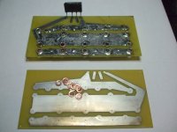
Yes 2oz copper.
The farthest MOSFET is 128mm from the output terminal.
The total output track is therefore 256mm with the terminal at or very close to the centreline.
PS tracks are both 127mm long.
I'm hoping there are not too many requests for further modifications.
It's getting close to time for ordering a batch to test.
One thing I don't have an idea of is the demand. How many to order??
I need to put a BOM together as well.
Andy
4 oz cooper
track lenght 127
Ambient 40 C
T rise 5
Current 13.6 A
Track resistance 0.0039
Vdrop 0.053
Power loss 0.73 Wats
Does not take much time to do this.
I understand the frustration one experience when the design is near the end (I have been in the same situation quite oten even at times to be told that there where mistakes on the skematics Just in case I was going to nick the design) a bit more effort and from what is already a realy realy prety board and you end up whith a realy good board
No bad for a couple of weeks work.
Last edited:
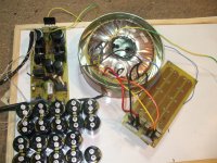
I've been thinking about the Power transformer.
For 2 x F5 v3 it looks like 800VA should be OK (Perhaps an Antek AN-8230 or similar).
Anybody comment on this?
I'm thinking about room im the chassis as the PSU board is 253mm x 80mm.
Andy
For 2 x F5 v3 it looks like 800VA should be OK (Perhaps an Antek AN-8230 or similar).
Anybody comment on this?
I'm thinking about room im the chassis as the PSU board is 253mm x 80mm.
Andy
- Status
- Not open for further replies.
- Home
- Amplifiers
- Pass Labs
- F5 Turbo Circuit Boards