thank you EUVL ! how can we redesign with different transistors ? nelson says simulations are not good enough..
Diomedian said:
The following paragraphs are a question, rather than a statement. 🙂
When using the Fairchild parts, the transconductance of the the P-channel parts is higher - so in the upper half of the circuit, you've got a lower S jfet and a higher S mosfet, and the lower half of the circuit you get a higher S jfet feeding a lower S mosfet, and these two combinations (partially?) cancel each other out.
Now when you're using the Toshiba mosfets, based on the fact that they're so well matched for transconductance, and that the jfets still aren't, you need to reduce the current output of the P-channel jfet (2sj74) and this is why you've increased source and feedback resistors.
Is this in the right ball park?
Thanks for the tips Patrick - I may end up going Fairchild unless I manage a bit better understanding here.
-j
you must look at amp as whole ....
besides xconductance , N and P type mozfets have different Ugs ;
that means that - chasing needed current and offset in/on output of amp - two pots will have different settings ............ so input Jfets will have different gains .
solution is simple .... ask Papa which THD gadget he's using ...... and what's good value of this horny resistor , for start

edit : writing about different xconductance - I have strictly IRFs on mind
Toshiba's are different animals

> Now when you're using the Toshiba mosfets, based on the fact that they're so well matched for transconductance, and that the jfets still aren't, .....
you need to reduce the effective transconductance of the P JFET by using a slightly larger source resistor. Once you have done that, of course you need to increase the feedback resistor as well to maintain the same closed loop gain.
At least that is my understanding.
> how can we redesign with different transistors ? nelson says simulations are not good enough..
I think I'll leave this question to the Master himself, if I may .....
> besides xconductance , N and P type mozfets have different Ugs ;
Not the case for Toshiba's. They have essentially the same Vgs for a particular current. That is the beauty, especially if you want to reduce the source resistor of the MOSFETs.
Patrick
EUVL said:> but these mosfets are expensive..can we try irf540 /9540 ?they are much cheaper...but maybe the circuit must be redesigned
Maybe you should just stick to the Fairchilds and the original Pass circuit.
You would not get the best from the Toshiba's unless you change the circuit to balance the open loop gain of the top half to the bottom half.
As to FETs being expensive, I wonder what % they cost compared to your finished amp with proper housings, heatsinks, power supplies, connectors, .......
Patrick
EUVL said:> you say you should change other things..can you show us redesigned f5 amp for 2sk1530/j201 ?
I can tell you off what I am using for my balanced version, but no guarantee for single ended :
Rail +/- 16V, 2A bias per MosFET
Source resistor 0R22
Gate resistor 100R
No thermistors, no current limiter (build at own risk !!!!)
Choose JFETs with Idss around 6.5mA.
For the 2SJ74 ONLY, change source resistor from 10R to 13R, and feedback resistor from 50R to 65R.
Patrick
Disclaimer :
Build at your own risk !!
thanks EUVL .. how can we redesign our amplifiers with different output transistors? Nelson said simulators are not good enough..
EUVL said:>.......
> besides xconductance , N and P type mozfets have different Ugs ;
Not the case for Toshiba's. They have essentially the same Vgs for a particular current. That is the beauty, especially if you want to reduce the source resistor of the MOSFETs.
Patrick
sorry - off course that I meant strictly on IRFs , but I forgot to write that .
> how can we redesign with different transistors ? nelson says simulations are not good enough..
I think I'll leave this question to the Master himself, if I may .....
> sorry - off course that I meant strictly on IRFs , but I forgot to write that .
Even worst for Fairchilds. And the transconductances differ by miles. You just need to roll back umteen pages for the measured data I published here. This is why the source resistor has to be such high value.
Of course one can compensate for all these things by clever design. I am just too lazy and rather use better matched (complementary) devices.
If only the JFETs would be just as good .....
Patrick
EUVL said:......
Of course one can compensate for all these things by clever design. .....
Patrick
that's easy ...... and well known - 100db of NFB
EUVL said:I thought you're a loyal Pass fan ??
Patrick

I'm too flippant to be anyone's loyal fan.....

(rispetto is totally another thing , btw . )
Bridged F5's
Jacco, you are no doubt correct - but I wasn't talking about altering the bias at all. The amp will easily put 2.5A into a 4 ohm load, unbridged, and 2.5A into an 8 ohm load bridged, but probably not in Class A and not steady state with music signals. Putting two F5s in parallel on each side of the bridge doubles the bias and will increase the Class A output point, but also doubles the part count, heat dissipation, yada-yada-yada. It would also probably give you an amp comparable to a DIY Pass X160. Maybe I need to order another four boards from Peter Daniel......
Each side of a bridged F5 pair biased at 2.5A means an idle dissipation of 57W for each output device (24V rails minus the voltage drop across 0.47 Ohm, times 2.5A)
You'll slow-fry both the output devices AND the 0.47 Ohm/3W resistors (0.47*2.5*2.5= ~3W )
Only way to safely up the bias on a bridged F5 is more output devices in parallel.
Easiest is just placing two F5's in parallel, the joy of the steep input impedance of JFETs and the ease with which they allow to be put in parallel. (in particular with degeneration)
200W in 4 Ohm is +7 Amps output current, just the drop of 3.3V across a 0.47 Ohm resistor will make the spec impossible to reach by bridging just a single pair of F5's. (same story with the 120W/8 talk)
Jacco, you are no doubt correct - but I wasn't talking about altering the bias at all. The amp will easily put 2.5A into a 4 ohm load, unbridged, and 2.5A into an 8 ohm load bridged, but probably not in Class A and not steady state with music signals. Putting two F5s in parallel on each side of the bridge doubles the bias and will increase the Class A output point, but also doubles the part count, heat dissipation, yada-yada-yada. It would also probably give you an amp comparable to a DIY Pass X160. Maybe I need to order another four boards from Peter Daniel......
dcb,
i already gathered that from your 50w post, mine was a addition to the question of the "smacking" Tea-Bag.
i already gathered that from your 50w post, mine was a addition to the question of the "smacking" Tea-Bag.
Bridged F5's
Jacco - cool. I think the last thing one wants to mess with is Papa's choice of the bias point on his selected MOSFETs.....my guess is Pass does a LOT of testing and listening to determine this, and I don't presume to think I can do any better.
I do think a "double-bridged" F5 would be a pretty cool project and would make one hell of an amplifier. In fact, given the simplicity of the circuit, ease of building these things and the high input impedance of the JFET's Pass has chosen, I suspect "scale-up" was an implicit design objective.
Zen Mod said:
if nothing else - go to Papa's site ( Pass Diy ) and download few pdfs ...
I mean that in "discrete OP for DIY " ( or something like that ) file you can find how to test jfets and mosfets .
use your imagination , and learn something ...... 😉
Thanks Zen Mod.
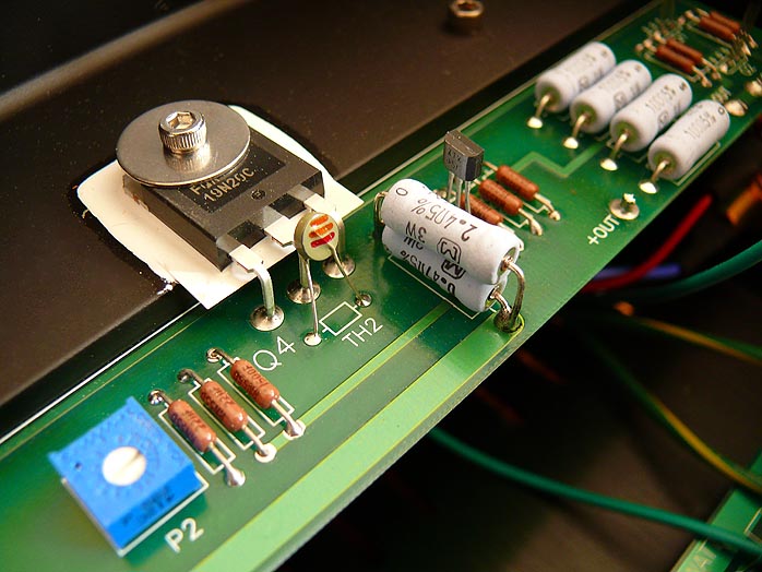
I'll build the jfet testing circuit and see what comes of it. I just thought someone might know right away if putting Q2 in backwards would fry it or not. Anyway.... I've ordered some more Q1 and Q2.
If Q1/2 check out ok on the test circuit I suppose the next step is to look at the current limiting parts. Test TH1/2. I'm a little concerned that I've actually used NTE128/129 instead of the ZTX450/550 (which is what mouser threw up for ZTX450/550 part). So that might also be the problem.
Thanks for the help.. will hope to do some testing tomorrow and will report back here with the results.
Fran
You can probably just take those current limiting parts out, replace the thermistors with 4.7k or so and see what happens. At least to eliminate those as sources of problem. After that, there aren't many parts left to go wrong 😉 Tom
Thanks Tom,
I know what you mean about the parts - thats why I was so p***ed off when I saw what I'd done!
Anyway, more investigations tomorrow. For tonight, its me and some Aretha, Otis and Carla Thomas. Chill out time!
Fran
I know what you mean about the parts - thats why I was so p***ed off when I saw what I'd done!
Anyway, more investigations tomorrow. For tonight, its me and some Aretha, Otis and Carla Thomas. Chill out time!
Fran
I was tapping and drilling on my F5 chassis tonight after a long day and decided it was time to just kick back and relax... lest I make a(nother) mistake  One more heatsink to go and hopefully fire it up with no smoke. The power supply with Christian's board and the AnTek toroid works just fine so far at +/-25 unloaded.
Just remember stuff happens to all of us. Hang in there. It should be easy to fix and it will be worth it!
One more heatsink to go and hopefully fire it up with no smoke. The power supply with Christian's board and the AnTek toroid works just fine so far at +/-25 unloaded. Just remember stuff happens to all of us. Hang in there. It should be easy to fix and it will be worth it!
woodturner-fran said:I just thought someone might know right away if putting Q2 in backwards would fry it or not.
If you check that link, you might think that it shouldn't: http://www.diyaudio.com/forums/showthread.php?postid=1202052#post1202052
Thanks Peter,
some testing to follow today. To be honest I'm kinda hoping that it is the problem! Otherwise theres another issue....
Fran
some testing to follow today. To be honest I'm kinda hoping that it is the problem! Otherwise theres another issue....
Fran
OK, so I done some more testing. First up was to check out Q1/Q2. I made up the circuit that someone posted a little back up here (Idss) - and I got 10mA for SJ74 and 9mA for SK170. So it would seem that they were alive still.
Next I decided to look at the current limiting circuit. I removed all the components from the circuit as detailed earlier in the thread. Now I found I could get the bias set ok across R11 and 12. Its set as 0.6V on both but my offset at the speaker terminals is high. The mosfets are heating up nicely, but they aren't that hot. I've left it on for a little while and will go back and check it again. The offset I'm seeing is "floating" ie moving around a good bit while the bias values seem pretty stable. I get 4.4-4.6V G-S on Q3 and 4 and I meaure 16V D to S on Q1 and 2.
Does this sound OK?
Fran
- Home
- Amplifiers
- Pass Labs
- F5 power amplifier